ZHCSEW6G
may 2013 – november 2020
DS90UB913A-Q1
PRODUCTION DATA
1
1
特性
2
应用
3
说明
4
Revision History
Device Comparison Table
5
Pin Configuration and Functions
Pin Functions: DS90UB913A-Q1 Serializer
6
Specifications
6.1
Absolute Maximum Ratings
6.2
ESD Ratings
6.3
Recommended Operating Conditions
6.4
Thermal Information
6.5
Electrical Characteristics
6.6
Recommended Serializer Timing For PCLK
6.7
AC Timing Specifications (SCL, SDA) - I2C-Compatible
6.8
Bidirectional Control Bus DC Timing Specifications (SCL, SDA) - I2C-Compatible
6.9
Timing Diagrams
6.10
Serializer Switching Characteristics
6.11
Typical Characteristics
7
Detailed Description
7.1
Overview
7.2
Functional Block Diagram
7.3
Feature Description
7.3.1
Serial Frame Format
7.3.2
Line Rate Calculations for the DS90UB913A/914A
7.3.3
Error Detection
7.3.4
Synchronizing Multiple Cameras
7.3.5
General Purpose I/O (GPIO) Descriptions
7.3.6
LVCMOS VDDIO Option
7.3.7
Pixel Clock Edge Select (TRFB / RRFB)
7.3.8
Power Down
7.4
Device Functional Modes
7.4.1
DS90UB913A/914A Operation with External Oscillator as Reference Clock
7.4.2
DS90UB913A/914A Operation with Pixel Clock from Imager as Reference Clock
7.4.3
MODE Pin on Serializer
7.4.4
Internal Oscillator
7.4.5
Built In Self Test
7.4.6
BIST Configuration and Status
7.4.7
Sample BIST Sequence
7.5
Programming
7.5.1
Programmable Controller
7.5.2
Description of Bidirectional Control Bus and I2C Modes
7.5.3
I2C Pass-Through
7.5.4
Slave Clock Stretching
7.5.5
ID[x] Address Decoder on the Serializer
7.5.6
Multiple Device Addressing
7.6
Register Maps
Application and Implementation
8.1
Application Information
8.1.1
Power Over Coax
8.1.2
Power-Up Requirements and PDB Pin
8.1.3
AC Coupling
8.1.4
Transmission Media
8.2
Typical Applications
8.2.1
Coax Application
8.2.1.1
Design Requirements
8.2.1.2
Detailed Design Procedure
8.2.1.3
Application Curves
8.2.2
STP Application
8.2.2.1
Design Requirements
8.2.2.2
Detailed Design Procedure
8.2.2.3
Application Curves
Power Supply Recommendations
8
Layout
8.1
Layout Guidelines
8.1.1
Interconnect Guidelines
8.2
Layout Example
9
Device and Documentation Support
9.1
Documentation Support
9.1.1
Related Documentation
9.2
Receiving Notification of Documentation Updates
9.3
Support Resources
9.4
Trademarks
Mechanical, Packaging, and Orderable Information
封装选项
机械数据 (封装 | 引脚)
RTV|32
MPQF166B
散热焊盘机械数据 (封装 | 引脚)
RTV|32
QFND448B
订购信息
zhcsew6g_oa
zhcsew6g_pm
8.2.2.3
Application Curves
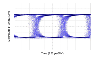
Figure 8-10
STP Eye Diagram at 1.4-Gbps Line Rate (100-MHz Pixel Clock) from Deserializer CML Loop-through Output (CMLOUT±)
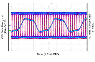
Figure 8-11
STP Eye Diagram with 100-MHz TX Pixel Clock Overlay from Deserializer CML Loop-through Output (CMLOUT±)
千亿体育app官网登录(中国)官方网站IOS/安卓通用版/手机APP
|
米乐app下载官网(中国)|ios|Android/通用版APP最新版
|
米乐|米乐·M6(中国大陆)官方网站
|
千亿体育登陆地址
|
华体会体育(中国)HTH·官方网站
|
千赢qy国际_全站最新版千赢qy国际V6.2.14安卓/IOS下载
|
18新利网v1.2.5|中国官方网站
|
bob电竞真人(中国官网)安卓/ios苹果/电脑版【1.97.95版下载】
|
千亿体育app官方下载(中国)官方网站IOS/安卓/手机APP下载安装
|