ZHCSEW6G may 2013 – november 2020 DS90UB913A-Q1
PRODUCTION DATA
- 1
- 1特性
- 2应用
- 3说明
- 4Revision History
- Device Comparison Table
- 5Pin Configuration and Functions
-
6Specifications
- 6.1 Absolute Maximum Ratings
- 6.2 ESD Ratings
- 6.3 Recommended Operating Conditions
- 6.4 Thermal Information
- 6.5 Electrical Characteristics
- 6.6 Recommended Serializer Timing For PCLK
- 6.7 AC Timing Specifications (SCL, SDA) - I2C-Compatible
- 6.8 Bidirectional Control Bus DC Timing Specifications (SCL, SDA) - I2C-Compatible
- 6.9 Timing Diagrams
- 6.10 Serializer Switching Characteristics
- 6.11 Typical Characteristics
- 7Detailed Description
- Application and Implementation
- Power Supply Recommendations
- 8Layout
- 9Device and Documentation Support
- Mechanical, Packaging, and Orderable Information
7.3.4 Synchronizing Multiple Cameras
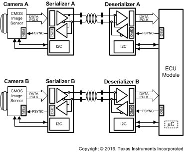
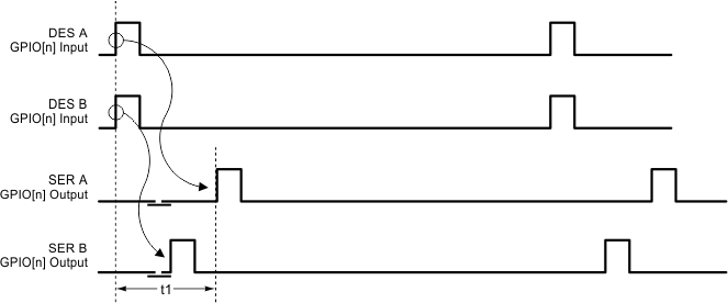
For applications requiring multiple cameras for frame-synchronization, it is recommended to utilize the General Purpose Input/Output (GPIO) pins to transmit control signals to synchronize multiple cameras together. To synchronize the cameras properly, the system controller needs to provide a field sync output (such as a vertical or frame sync signal) and the cameras must be set to accept an auxiliary sync input. The vertical synchronize signal corresponds to the start and end of a frame and the start and end of a field. Note this form of synchronization timing relationship has a non-deterministic latency. After the control data is reconstructed from the bidirectional control channel, there will be a time variation of the GPIO signals arriving at the different target devices (between the parallel links). The maximum latency delta (t1) of the GPIO data transmitted across multiple links is 25 µs.
The user must verify that the timing variations between the different links are within their system and timing specifications.
See Figure 7-1 for an example of this function.
The maximum time (t1) between the rising edge of GPIO (that is, sync signal) to the time the signal arrives at Camera A and Camera B is 25 µs.
 Figure 7-1 Synchronizing Multiple Cameras
 Figure 7-2 GPIO Delta Latency