ZHCSEW6G may 2013 – november 2020 DS90UB913A-Q1
PRODUCTION DATA
- 1
- 1特性
- 2应用
- 3说明
- 4Revision History
- Device Comparison Table
- 5Pin Configuration and Functions
-
6Specifications
- 6.1 Absolute Maximum Ratings
- 6.2 ESD Ratings
- 6.3 Recommended Operating Conditions
- 6.4 Thermal Information
- 6.5 Electrical Characteristics
- 6.6 Recommended Serializer Timing For PCLK
- 6.7 AC Timing Specifications (SCL, SDA) - I2C-Compatible
- 6.8 Bidirectional Control Bus DC Timing Specifications (SCL, SDA) - I2C-Compatible
- 6.9 Timing Diagrams
- 6.10 Serializer Switching Characteristics
- 6.11 Typical Characteristics
- 7Detailed Description
- Application and Implementation
- Power Supply Recommendations
- 8Layout
- 9Device and Documentation Support
- Mechanical, Packaging, and Orderable Information
7.5.2 Description of Bidirectional Control Bus and I2C Modes
The I2C-compatible interface allows programming of the DS90UB913A-Q1, DS90UB914A-Q1, or an external remote device (such as image sensor) through the bidirectional control channel. Register programming transactions to/from the DS90UB913A-Q1/914A-Q1 chipset are employed through the clock (SCL) and data (SDA) lines. These two signals have open drain I/Os and both lines must be pulled-up to VDDIO by an external resistor. Pullup resistors or current sources are required on the SCL and SDA busses to pull them high when they are not being driven low. A logic LOW is transmitted by driving the output low. Logic HIGH is transmitted by releasing the output and allowing it to be pulled-up externally. The appropriate pullup resistor values will depend upon the total bus capacitance and operating speed. The DS90UB913A I2C bus data rate supports up to 400 kbps according to I2C fast mode specifications.
For further description of general I2C communication, please refer to application note Understanding the I2C Bus (SLVA704). For more information on choosing appropriate pullup resistor values, please refer to application note I2C Bus Pullup Resistor Calculation (SLVA689).
 Figure 7-9 Write Byte
 Figure 7-10 Read Byte
 Figure 7-11 Basic Operation
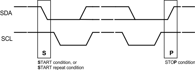
 Figure 7-12 Start and Stop Conditions