ZHCSEW6G may 2013 – november 2020 DS90UB913A-Q1
PRODUCTION DATA
- 1
- 1特性
- 2应用
- 3说明
- 4Revision History
- Device Comparison Table
- 5Pin Configuration and Functions
-
6Specifications
- 6.1 Absolute Maximum Ratings
- 6.2 ESD Ratings
- 6.3 Recommended Operating Conditions
- 6.4 Thermal Information
- 6.5 Electrical Characteristics
- 6.6 Recommended Serializer Timing For PCLK
- 6.7 AC Timing Specifications (SCL, SDA) - I2C-Compatible
- 6.8 Bidirectional Control Bus DC Timing Specifications (SCL, SDA) - I2C-Compatible
- 6.9 Timing Diagrams
- 6.10 Serializer Switching Characteristics
- 6.11 Typical Characteristics
- 7Detailed Description
- Application and Implementation
- Power Supply Recommendations
- 8Layout
- 9Device and Documentation Support
- Mechanical, Packaging, and Orderable Information
8.2 Layout Example
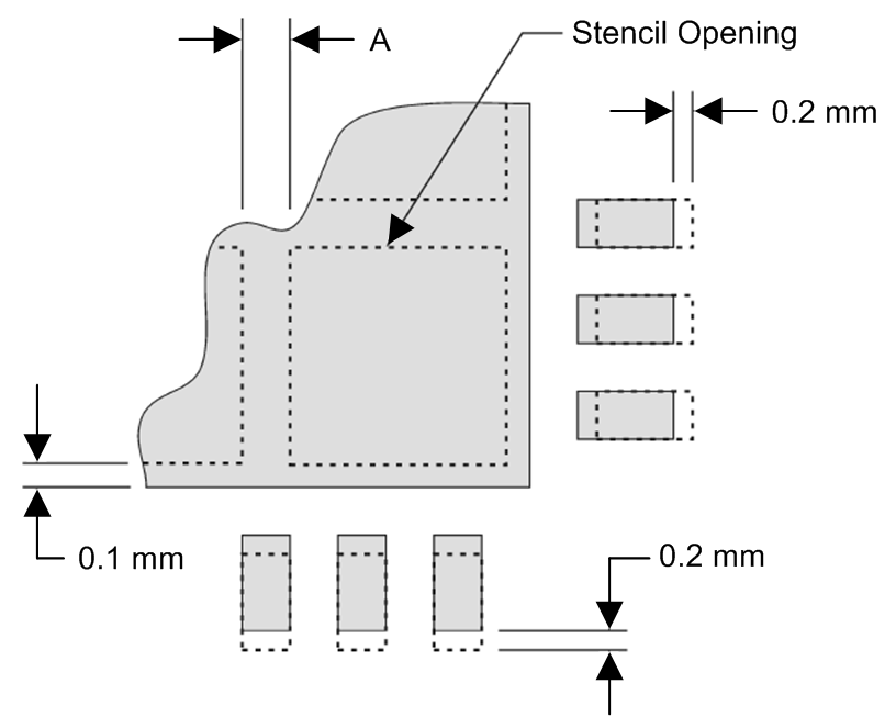
Stencil parameters such as aperture area ratio and the fabrication process have a significant impact on paste deposition. Inspection of the stencil prior to placement of the WQFN package is highly recommended to improve board assembly yields. If the via and aperture openings are not carefully monitored, the solder may flow unevenly through the DAP. Stencil parameters for aperture opening and via locations are shown below:
 Figure 8-1 No Pullback WQFN, Single Row Reference Diagram
| DEVICE | PIN COUNT | MKT DWG | PCB I/O PAD SIZE (mm) | PCB PITCH (mm) | PCB DAP SIZE(mm) | STENCIL I/O APERTURE (mm) | STENCIL DAP APERTURE (mm) | NUMBER OF DAP APERTURE OPENINGS | GAP BETWEEN DAP APERTURE (Dim A mm) |
|---|---|---|---|---|---|---|---|---|---|
| DS90UB913A-Q1 | 32 | RTV | 0.25 x 0.6 | 0.5 | 3.1 x 3.1 | 0.25 x 0.7 | 1.4 x 1.4 | 4 | 0.2 |
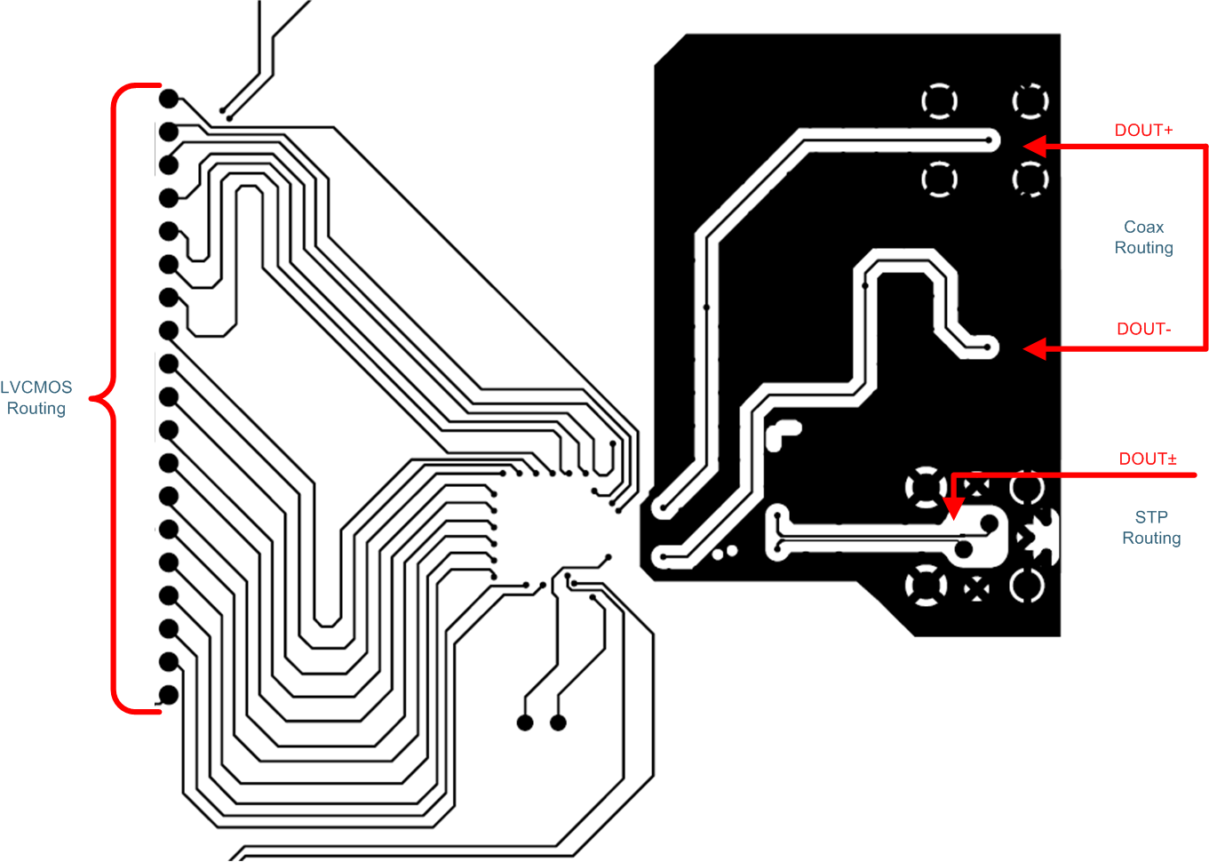
 Figure 8-2 DS90UB913A-Q1 Serializer Example Layout
The following PCB layout examples are derived from the layout design of the DS90UB913A-Q1 Evaluation Module (DS90UB913A-CXEVM and DS90UB914A-CXEVM REV A User’s Guide). These graphics and additional layout description are used to demonstrate both proper routing and proper solder techniques when designing in this Serializer.