ZHCSEY4 April 2016 DS90UB924-Q1
PRODUCTION DATA.
- 1 特性
- 2 应用范围
- 3 说明
- 4 修订历史记录
- 5 Pin Configuration and Functions
-
6 Specifications
- 6.1 Absolute Maximum Ratings
- 6.2 ESD Ratings
- 6.3 Recommended Operating Conditions
- 6.4 Thermal Information
- 6.5 DC Electrical Characteristics
- 6.6 AC Electrical Characteristics
- 6.7 DC and AC Serial Control Bus Characteristics
- 6.8 Timing Requirements for the Serial Control Bus
- 6.9 Timing Requirements
- 6.10 Typical Characteristics
-
7 Detailed Description
- 7.1 Overview
- 7.2 Functional Block Diagram
- 7.3
Feature Description
- 7.3.1 High-Speed Forward Channel Data Transfer
- 7.3.2 Low-Speed Back Channel Data Transfer
- 7.3.3 Backward Compatible Mode
- 7.3.4 Input Equalization
- 7.3.5 Common Mode Filter Pin (CMF)
- 7.3.6 Power Down (PDB)
- 7.3.7 Video Control Signals
- 7.3.8 EMI Reduction Features
- 7.3.9 Built In Self Test (BIST)
- 7.3.10 Internal Pattern Generation
- 7.3.11 Serial Link Fault Detect
- 7.3.12 Oscillator Output
- 7.3.13 Interrupt Pin (INTB / INTB_IN)
- 7.3.14 General-Purpose I/O
- 7.3.15 I2S Audio Interface
- 7.3.16 AV Mute Prevention
- 7.3.17 OEN Toggling Limitation
- 7.4 Device Functional Modes
- 7.5 Programming
- 7.6 Register Maps
- 8 Application and Implementation
- 9 Power Supply Recommendations
- 10Layout
- 11器件和文档支持
- 12机械、封装和可订购信息
7 Detailed Description
7.1 Overview
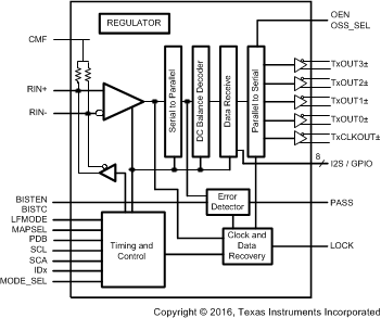
The DS90UB924-Q1 receives a 35-bit symbol over a single serial FPD-Link III pair operating at up to 3.36 Gbps line rate and converts this stream into an FPD-Link (OpenLDI) Interface (4 LVDS data channels + 1 LVDS Clock). The FPD-Link III serial stream contains an embedded clock, video control signals, and the DC-balanced video data and audio data which enhance signal quality to support AC coupling.
The DS90UB924-Q1 deserializer attains lock to a data stream without the use of a separate reference clock source, which greatly simplifies system complexity and overall cost. The deserializer also synchronizes to the serializer regardless of the data pattern, delivering true automatic plug and lock performance. It can lock to the incoming serial stream without the need of special training patterns or sync characters. The deserializer recovers the clock and data by extracting the embedded clock information, validating then deserializing the incoming data stream.
The DS90UB924-Q1 deserializer incorporates an I2C-compatible interface. The I2C-compatible interface allows programming of serializer or deserializer devices from a local host controller. In addition, the serializer/deserializer devices incorporate a bidirectional control channel (BCC) that allows communication between serializer/deserializer as well as remote I2C slave devices.
The bidirectional control channel (BCC) is implemented via embedded signaling in the high-speed forward channel (serializer to deserializer) combined with lower speed signaling in the reverse channel (deserializer to serializer). Through this interface, the BCC provides a mechanism to bridge I2C transactions across the serial link from one I2C bus to another. The implementation allows for arbitration with other I2C compatible masters at either side of the serial link.
The DS90UB924-Q1 deserializer is intended for use with DS90UB921-Q1, DS90UB925Q-Q1, or DS90UB927Q-Q1 serializers, but is also backward compatible with DS90UR905Q and DS90UR907Q FPD-Link III serializers.
7.2 Functional Block Diagram
7.3 Feature Description
7.3.1 High-Speed Forward Channel Data Transfer
The high-speed Forward Channel is composed of a 35-bit frame containing video data, sync signals, I2C, and I2S audio transmitted from serializer to deserializer. Figure 19 shows the serial stream PCLK cycle. This data payload is optimized for signal transmission over an AC-coupled link. Data is randomized, DC-balanced and scrambled.
 Figure 19. FPD-Link III Serial Stream
The device supports pixel clock ranges of 5 MHz to 15 MHz (LFMODE=1) and 15 MHz to 96 MHz (LFMODE=0). This corresponds to an application payload rate range of 155 Mbps to 2.976 Gbps, with an actual line rate range of 525 Mbps to 3.36 Gbps.
7.3.2 Low-Speed Back Channel Data Transfer
The low-speed back channel of the DS90UB924-Q1 provides bidirectional communication between the display and host processor. The back channel control data is transferred over the single serial link along with the high-speed forward data, DC balance coding, and embedded clock information. Together, the forward channel and back channel form the bidirectional control channel (BCC). This architecture provides a backward path across the serial link together with a high speed forward channel. The back channel contains the I2C, CRC and 4 bits of standard GPIO information with 10 Mbps line rate.
7.3.3 Backward Compatible Mode
The DS90UB924-Q1 is also backward compatible to the DS90UR905Q and DS90UR907Q for PCLK frequencies ranging from 15 MHz to 65 MHz. The deserializer receives 28 bits of data over a single serial FPD-Link III pair operating at a payload rate of 120 Mbps to 1.8 Gbps, corresponding to a line rate of 140 Mbps to 2.1 Gbps. The backward compatibility configuration can be selected through the MODE_SEL pin or programmed through the device control registers (Table 8). The bidirectional control channel, bidirectional GPIOs, I2S, and interrupt (INTB) are not active in this mode. However, local I2C access to the serializer is still available.
7.3.4 Input Equalization
An FPD-Link III input adaptive equalizer provides compensation for transmission medium losses and reduces medium-induced deterministic jitter.
The adaptive equalizer may be set to a Long Cable Mode (LCBL), using the MODE_SEL pin (Table 6). This mode is typically used with longer cables where it may be desirable to start adaptive equalization from a higher default gain. In this mode, the device attempts to lock from a minimum floor AEQ value, defined by a value stored in the control registers (Table 8).
7.3.5 Common Mode Filter Pin (CMF)
The deserializer provides access to the center tap of the internal CML termination. A 0.1 μF capacitor must be connected from this pin to GND for additional common-mode filtering of the differential pair (Figure 37). This increases noise rejection capability in high-noise environments.
7.3.6 Power Down (PDB)
The deserializer has a PDB input pin to enable or power down the device. This pin may be controlled by an external device, or through VDDIO, where VDDIO = 3 V to 3.6 V or VDD33. To save power, disable the link when the display is not needed (PDB = LOW). Ensure that this pin is not driven HIGH before VDD33 and VDDIO have reached final levels. When PDB is driven low, ensure that the pin is driven to 0 V for at least 1.5 ms before releasing or driving high (See Recommended Operating Conditions ). If the PDB is pulled up to VDDIO = 3.0 V to 3.6 V or VDD33 directly, a 10 kΩ pullup resistor and a >10 µF capacitor to ground are required (See Figure 37).
Toggling PDB low POWER DOWN the device and RESET all control registers to default. During this time, PDB must be held low for a minimum of 2 ms (see AC Electrical Characteristics).
7.3.7 Video Control Signals
The video control signal bits embedded in the high-speed FPD-Link (OpenLDI) LVDS are subject to certain limitations relative to the video pixel clock period (PCLK). By default, the device applies a minimum pulse width filter on these signals to help eliminate spurious transitions.
Normal Mode Control Signals (VS, HS, DE) have the following restrictions:
- Horizontal Sync (HS): The video control signal pulse width must be 3 PCLKs or longer when the Control Signal Filter (register bit 0x03[4]) is enabled (default). Disabling the Control Signal Filter removes this restriction (minimum is 1 PCLK). See Table 8. HS can have at most two transitions per 130 PCLKs.
- Vertical Sync (VS): The video control signal pulse is limited to 1 transition per 130 PCLKs. Thus, the minimum pulse width is 130 PCLKs.
- Data Enable Input (DE): The video control signal pulse width must be 3 PCLKs or longer when the Control Signal Filter (register bit 0x03[4]) is enabled (default). Disabling the Control Signal Filter removes this restriction (minimum is 1 PCLK). See Table 8. DE can have at most two transitions per 130 PCLKs.
7.3.8 EMI Reduction Features
7.3.8.1 LVCMOS VDDIO Option
The 1.8 V/3.3 V LVCMOS inputs and outputs are powered from a separate VDDIO supply pin to offer compatibility with external system interface signals. Note: When configuring the VDDIO power supplies, all the single-ended control input pins (except PDB) for device need to scale together with the same operating VDDIO levels. If VDDIO is selected to operate in the 3.0 V to 3.6 V range, VDDIO must be operated within 300 mV of VDD33 (See Recommended Operating Conditions).
7.3.9 Built In Self Test (BIST)
An optional At-speed Built-In Self Test (BIST) feature supports testing of the high-speed serial link and the low-speed back channel without external data connections. This is useful in the prototype stage, equipment production, in-system test, and system diagnostics.
7.3.9.1 BIST Configuration and Status
The BIST mode is enabled at the deserializer by pin (BISTEN) or BIST configuration register. The test may select either an external PCLK or the 33 MHz internal oscillator clock (OSC) frequency. In the absence of PCLK, the user can select the internal OSC frequency at the deserializer through the BISTC pin or BIST configuration register.
When BIST is activated at the deserializer, a BIST enable signal is sent to the serializer through the back channel. The serializer outputs a test pattern and drives the link at speed. The deserializer detects the test pattern and monitors it for errors. The deserializer PASS output pin toggles to flag each frame received containing one or more errors. The serializer also tracks errors indicated by the CRC fields in each back channel frame.
The BIST status can be monitored real time on the deserializer PASS pin, with each detected error resulting in a half pixel clock period toggled LOW. After BIST is deactivated, the result of the last test is held on the PASS output until reset (new BIST test or Power Down). A high on PASS indicates NO ERRORS were detected. A Low on PASS indicates one or more errors were detected. The duration of the test is controlled by the pulse width applied to the deserializer BISTEN pin. LOCK status is valid throughout the entire duration of BIST.
See Figure 20 for the BIST mode flow diagram.
7.3.9.1.1 Sample BIST Sequence
- BIST Mode is enabled via the BISTEN pin of Deserializer. The desired clock source is selected through the deserializer BISTC pin.
- The serializer is awakened through the back channel if it is not already on. An all zeros pattern is balanced, scrambled, randomized, and sent through the FPD-Link III interface to the deserializer. Once the serializer and the deserializer are in BIST mode and the deserializer acquires LOCK, the PASS pin of the deserializer goes high, and BIST starts checking the data stream. If an error in the payload (1 to 35) is detected, the PASS pin switches low for one half of the clock period. During the BIST test, the PASS output can be monitored and counted to determine the payload error rate.
- To stop BIST mode, set the BISTEN pin LOW. The deserializer stops checking the data, and the final test result is held on the PASS pin. If the test ran error free, the PASS output remains HIGH. If there one or more errors were detected, the PASS output outputs constant LOW. The PASS output state is held until a new BIST is run, the device is RESET, or the device is powered down. BIST duration is user-controlled and may be of any length.
The link returns to normal operation after the deserializer BISTEN pin is low. Figure 21 shows the waveform diagram of a typical BIST test for two cases. Case 1 is error free, and Case 2 shows one with multiple errors. In most cases it is difficult to generate errors due to the robustness of the link (differential data transmission, and so forth.), thus they may be introduced by greatly extending the cable length, faulting the interconnect medium, or reducing signal condition enhancements (Rx equalization).
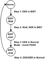 Figure 20. BIST Mode Flow Diagram
7.3.9.2 Forward Channel and Back Channel Error Checking
The deserializer, on locking to the serial stream, compares the recovered serial stream with all zeroes and records any errors in status registers. Errors are also dynamically reported on the PASS pin of the deserializer. Forward channel errors may also be read from register 0x25 ( Table 8).
The back-channel data is checked for CRC errors once the serializer locks onto the back-channel serial stream, as indicated by link detect status (register bit 0x1C[0] - Table 8). CRC errors are recorded in an 8-bit register in the deserializer. The register is cleared when the serializer enters the BIST mode. As soon as the serializer enters BIST mode, the functional mode CRC register starts recording any back channel CRC errors. The BIST mode CRC error register is active in BIST mode only and keeps the record of the last BIST run until cleared or the serializer enters BIST mode again.
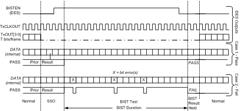 Figure 21. BIST Waveforms
7.3.10 Internal Pattern Generation
The DS90UB924-Q1 deserializer features an internal pattern generator. It allows basic testing and debugging of an integrated panel. The test patterns are simple and repetitive and allow for a quick visual verification of panel operation. As long as the device is not in power down mode, the test pattern is displayed even if no input is applied. If no clock is received, the test pattern can be configured to use a programmed oscillator frequency. For detailed information, refer to TI Application Note: (AN-2198).
7.3.10.1 Pattern Options
The DS90UB924-Q1 deserializer pattern generator is capable of generating 17 default patterns for use in basic testing and debugging of panels. Each pattern can be inverted using register bits (see Table 8). The 17 default patterns are listed as follows:
- White/Black (default/inverted)
- Black/White
- Red/Cyan
- Green/Magenta
- Blue/Yellow
- Horizontally Scaled Black to White/White to Black
- Horizontally Scaled Black to Red/Cyan to White
- Horizontally Scaled Black to Green/Magenta to White
- Horizontally Scaled Black to Blue/Yellow to White
- Vertically Scaled Black to White/White to Black
- Vertically Scaled Black to Red/Cyan to White
- Vertically Scaled Black to Green/Magenta to White
- Vertically Scaled Black to Blue/Yellow to White
- Custom Color / Inverted configured in PGRS
- Black-White/White-Black Checkerboard (or custom checkerboard color, configured in PGCTL)
- YCBR/RBCY VCOM pattern, orientation is configurable from PGCTL
- Color Bars (White, Yellow, Cyan, Green, Magenta, Red, Blue, Black) – Note: not included in the auto-scrolling feature
7.3.10.2 Color Modes
By default, the Pattern Generator operates in 24-bit color mode, where all bits of the red, green, and blue outputs are enabled. 18-bit color mode can be activated from the configuration registers (Table 8). In 18-bit mode, the 6 most significant bits (bits 7-2) of the Red, Green, and Blue outputs are enabled; the 2 least significant bits are 0.
7.3.10.3 Video Timing Modes
The Pattern Generator has two video timing modes – external and internal. In external timing mode, the Pattern Generator detects the video frame timing present on the DE and VS inputs. If Vertical Sync signaling is not present on VS, the Pattern Generator determines Vertical Blank by detecting when the number of inactive pixel clocks (DE = 0) exceeds twice the detected active line length. In internal timing mode, the Pattern Generator uses custom video timing as configured in the control registers. The internal timing generation may also be driven by an external clock. By default, external timing mode is enabled. Internal timing or Internal timing with External Clock are enabled by the control registers (Table 8). If internal clock generation is used, register 0x39 bit 1 must be set.
7.3.10.4 External Timing
In external timing mode, the pattern generator passes the incoming DE, HS, and VS signals unmodified to the video control outputs after a two-pixel clock delay. It extracts the active frame dimensions from the incoming signals in order to properly scale the brightness patterns. If the incoming video stream does not use the VS signal, the Pattern Generator determines the Vertical Blank time by detecting a long period of pixel clocks without DE asserted.
7.3.10.5 Pattern Inversion
The Pattern Generator also incorporates a global inversion control, located in the PGCFG register, which causes the output pattern to be bitwise-inverted. For example, the full-screen Red pattern becomes full-screen cyan, and the Vertically Scaled Black to Green pattern becomes Vertically Scaled White to Magenta.
7.3.10.6 Auto Scrolling
The Pattern Generator supports an Auto-Scrolling mode, in which the output pattern cycles through a list of enabled pattern types. A sequence of up to 16 patterns may be defined in the registers. The patterns may appear in any order in the sequence and may also appear more than once.
7.3.11 Serial Link Fault Detect
The DS90UB924-Q1 can detect fault conditions in the FPD-Link III interconnect. If a fault condition occurs, the Link Detect Status is 0 (cable is not detected) on bit 0 of address 0x1C (Table 8). The device detects any of the following conditions:
- Cable open
- RIN+ to - short
- RIN+ to GND short
- RIN- to GND short
- RIN+ to battery short
- RIN- to battery short
- Cable is linked incorrectly (RIN+/RIN- connections reversed)
NOTE
The device detects any of the above conditions, but does not report specifically which one has occurred.
7.3.12 Oscillator Output
The deserializer provides an optional TxCLKOUT± output when the input clock (serial stream) has been lost. This is based on an internal oscillator and may be controlled from register 0x02, bit 5 (OSC Clock Output Enable) Table 8.
7.3.13 Interrupt Pin (INTB / INTB_IN)
- Read HDCP_ISR Register 0xC7. (Table 8)
- On the serializer, set register (ICR) 0xC6[5] = 1 and 0xC6[0] = 1 to configure the interrupt.
- On the serializer, read from ISR register 0xC7 to arm the interrupt for the first time.
- When INTB_IN is set LOW, the INTB pin on the serializer also pulls low, indicating an interrupt condition.
- The external controller detects INTB = LOW and reads the ISR register to determine the interrupt source. Reading this register also clears and resets the interrupt.
The INTB_IN signal is sampled and required approximately 8.6 μs of the minimum setup and hold time.
8.6 μs = 30 bit per back channel frame / (5 Mbps rate × ±30% Variation) = 30 / (5E6 × 0.7)
Note that -30% is the worst case.
7.3.14 General-Purpose I/O
7.3.14.1 GPIO[3:0]
In normal operation, GPIO[3:0] may be used as general purpose IOs in either forward channel (outputs) or back channel (inputs) mode. GPIO modes may be configured from the registers (Table 8). GPIO[1:0] are dedicated pins and GPIO[3:2] are shared with I2S_DC and I2S_DD respectively. Note: if the DS90UB924-Q1 is paired with a DS90UB921-Q1 or DS90UB925Q-Q1 serializer, the devices must be configured into 18-bit mode to allow usage of GPIO pins on the serializer. To enable 18-bit mode, set serializer register 0x12[2] = 1. 18-bit mode is auto-loaded into the deserializer from the serializer. See Table 1 for GPIO enable and configuration.
Table 1. DS90UB921-Q1/DS90UB925Q-Q1 GPIO Enable and Configuration
| DESCRIPTION | DEVICE | FORWARD CHANNEL | BACK CHANNEL |
|---|---|---|---|
| GPIO3 | DS90UB921-Q1/ DS90UB925Q-Q1 | 0x0F = 0x03 | 0x0F = 0x05 |
| DS90UB924-Q1 | 0x1F = 0x05 | 0x1F = 0x03 | |
| GPIO2 | DS90UB921-Q1/ DS90UB925Q-Q1 | 0x0E = 0x30 | 0x0E = 0x50 |
| DS90UB924-Q1 | 0x1E = 0x50 | 0x1E = 0x30 | |
| GPIO1/GPIO1 (SER/DES) |
DS90UB921-Q1/ DS90UB925Q-Q1 | N/A | 0x0E = 0x05 |
| DS90UB924-Q1 | N/A | 0x1E = 0x03 | |
| GPO_REG5/GPIO1 (SER/DES) |
DS90UB921-Q1/ DS90UB925Q-Q1 | 0x10 = 0x03 | N/A |
| DS90UB924-Q1 | 0x1E = 0x05 | N/A | |
| GPIO0/GPIO0 (SER/DES) |
DS90UB921-Q1/ DS90UB925Q-Q1 | N/A | 0x0D = 0x05 |
| DS90UB924-Q1 | N/A | 0x1D = 0x03 | |
| GPO_REG4/GPIO0 (SER/DES) |
DS90UB921-Q1/ DS90UB925Q-Q1 | 0x0F = 0x30 | N/A |
| DS90UB924-Q1 | 0x1D = 0x05 | N/A |
Table 2. DS90UB927Q-Q1 GPIO Enable and Configuration
| DESCRIPTION | DEVICE | FORWARD CHANNEL | BACK CHANNEL |
|---|---|---|---|
| GPIO3 | DS90UB927Q-Q1 | 0x0F = 0x03 | 0x0F = 0x05 |
| DS90UB924-Q1 | 0x1F = 0x05 | 0x1F = 0x03 | |
| GPIO2 | DS90UB927Q-Q1 | 0x0E = 0x30 | 0x0E = 0x50 |
| DS90UB924-Q1 | 0x1E = 0x50 | 0x1E = 0x30 | |
| GPIO1 | DS90UB927Q-Q1 | 0x0E = 0x03 | 0x0E = 0x05 |
| DS90UB924-Q1 | 0x1E = 0x05 | 0x1E = 0x03 | |
| GPIO0 | DS90UB927Q-Q1 | 0x0D = 0x03 | 0x0D = 0x05 |
| DS90UB924-Q1 | 0x1D = 0x05 | 0x1D = 0x03 |
Note: GPO_REG4 of the DS90UB921-Q1 or DS90UB925-Q1 can be used as a forward channel GPIO, outputting on GPIO0 of DS90UB924-Q1. This can be set as follows:
- Set DS90UB921-Q1 or DS90UB925-Q1 in 18-bit mode by mode pin = 1 or by register 0x12[2] = 1.
- Set DS90UB924-Q1 register 0x1D[0] = 1 and 0x1D[2] = 1; this will enable GPIO0 of DS90UB924-Q1 as output.
- Set DS90UB921-Q1 or DS90UB925-Q1 register 0x0F[4] = 1 and 0x0F[5] = 1; this will enable GPO_REG4 of DS90UB921-Q1 or DS90UB925-Q1 as input.
Similarly GPO_REG5 of DS90UB921-Q1 or DS90UB925-Q1 can output to GPIO1 of DS90UB924-Q1:
- Set DS90UB921-Q1 or DS90UB925-Q1 in 18-bit mode by mode pin = 1 or by register 0x12[2] = 1.
- Set DS90UB924-Q1 register 0x1E[0] = 1 and 0x1E[2] = 1; this will enable GPIO1 of DS90UB924-Q1 as output.
- Set DS90UB921-Q1 or DS90UB925-Q1 register 0x10[0] = 1 and 0x10[1] = 1; this will enable GPO_REG5 DS90UB921-Q1 or DS90UB925-Q1 as input.
The input value present on GPIO[3:0] may also be read from register or configured to local output mode (Table 8).
7.3.14.2 GPIO[8:5]
GPIO_REG[8:5] are register-only GPIOs and may be programmed as outputs or read as inputs through local register bits only. Where applicable, these bits are shared with I2S pins and override I2S input if enabled into GPIO_REG mode. See Table 3 for GPIO enable and configuration.
Note: Local GPIO value may be configured and read either through local register access, or remote register access through the Low-Speed Bidirectional Control Channel. Configuration and state of these pins are not transported from serializer to deserializer as is the case for GPIO[3:0].
Table 3. GPIO_REG and GPIO Local Enable and Configuration
| DESCRIPTION | REGISTER CONFIGURATION | FUNCTION |
|---|---|---|
| GPIO_REG8 | 0x21 = 0x01 | Output, L |
| 0x21 = 0x09 | Output, H | |
| 0x21 = 0x03 | Input, Read: 0x6F[0] | |
| GPIO_REG7 | 0x21 = 0x01 | Output, L |
| 0x21 = 0x09 | Output, H | |
| 0x21 = 0x03 | Input, Read: 0x6E[7] | |
| GPIO_REG6 | 0x20 = 0x01 | Output, L |
| 0x20 = 0x09 | Output, H | |
| 0x20 = 0x03 | Input, Read: 0x6E[6] | |
| GPIO_REG5 | 0x20 = 0x01 | Output, L |
| 0x20 = 0x09 | Output, H | |
| 0x20 = 0x03 | Input, Read: 0x6E[5] | |
| GPIO3 | 0x1F = 0x01 | Output, L |
| 0x1F = 0x09 | Output, H | |
| 0x1F = 0x03 | Input, Read: 0x6E[3] | |
| GPIO2 | 0x1E = 0x01 | Output, L |
| 0x1E = 0x09 | Output, H | |
| 0x1E = 0x03 | Input, Read: 0x6E[2] | |
| GPIO1 | 0x1E = 0x01 | Output, L |
| 0x1E = 0x09 | Output, H | |
| 0x1E = 0x03 | Input, Read: 0x6E[1] | |
| GPIO0 | 0x1D = 0x01 | Output, L |
| 0x1D = 0x09 | Output, H | |
| 0x1D = 0x03 | Input, Read: 0x6E[0] |
7.3.15 I2S Audio Interface
The DS90UB924-Q1 deserializer features six I2S output pins that, when paired with a DS90UB927Q-Q1 serializer, supports surround-sound audio applications. The bit clock (I2S_CLK) supports frequencies between 1 MHz and the smaller of < PCLK/4 or < 13 MHz. Four I2S data outputs carry two channels of I2S-formatted digital audio each, with each channel delineated by the word select (I2C_WC) input. The I2S audio interface is not available in Backwards Compatibility Mode (BKWD = 1).
 Figure 22. I2S Connection Diagram
 Figure 23. I2S Frame Timing Diagram
When paired with a DS90UB921-Q1 or DS90UB925Q-Q1, the DS90UB924-Q1 I2S interface supports a single I2S data output through I2S_DA (24-bit video mode), or two I2S data outputs through I2S_DA and I2S_DB (18-bit video mode).
7.3.15.1 I2S Transport Modes
By default, packetized audio is received during video blanking periods in dedicated data island transport frames. The transport mode is set in the serializer and auto-loaded into the deserializer by default. The audio configuration may be disabled from control registers if Forward Channel Frame Transport of I2S data is desired. In frame transport, only I2S_DA is received to the DS90UB924-Q1 deserializer. Surround Sound Mode, which transmits all four I2S data inputs (I2S_D[D:A]), may only be operated in Data Island Transport mode. This mode is only available when connected to a DS90UB927Q-Q1 serializer. If connected to a DS90UB921-Q1 or DS90UB925Q-Q1 serializer, only I2S_DA and I2S_DB may be received.
7.3.15.2 I2S Repeater
I2S audio may be fanned-out and propagated in the repeater application. By default, data is propagated via data island transport on the FPD-Link (OpenLDI) interface during the video blanking periods. If frame transport is desired, connect the I2S pins from the deserializer to all serializers. Activating surround sound at the top-level serializer automatically configures downstream serializers and deserializers for surround-sound transport utilizing Data Island Transport. If 4-channel operation utilizing I2S_DA and I2S_DB only is desired, this mode must be explicitly set in each serializer and deserializer control register throughout the repeater tree (Table 8).
A DS90UB924-Q1 deserializer configured in repeater mode may also regenerate I2S audio from its I2S input pins in lieu of Data Island frames. See Figure 31 and the I2C control registers (Table 8) for additional details.
7.3.15.3 I2S Jitter Cleaning
The DS90UB924-Q1 features a standalone PLL to clean the I2S data jitter, supporting high-end car audio systems. If I2S_CLK frequency is less than 1 MHz, this feature must be disabled through register 0x2B[7]. See Table 8.
7.3.15.4 MCLK
The deserializer has an I2S Master Clock Output (MCLK). It supports ×1, ×2, or ×4 of I2S CLK Frequency. When the I2S PLL is disabled, the MCLK output is off. Table 4 covers the range of I2S sample rates and MCLK frequencies. By default, all the MCLK output frequencies are ×2 of the I2S CLK frequencies. The MCLK frequencies can also be enabled through the register bits 0x3A[6:4] (I2S DIVSEL), shown in Table 8. To select desired MCLK frequency, write 0x3A[7], then write to bit [6:4] accordingly.
Table 4. Audio Interface Frequencies
| SAMPLE RATE (kHz) | I2S DATA WORD SIZE (BITS) | I2S_CLK (MHz) | MCLK OUTPUT (MHz) | REGISTER 0x3A[6:4]'b |
|---|---|---|---|---|
| 32 | 16 | 1.024 | I2S_CLK x1 | 000 |
| I2S_CLK x2 | 001 | |||
| I2S_CLK x4 | 010 | |||
| 44.1 | 1.4112 | I2S_CLK x1 | 000 | |
| I2S_CLK x2 | 001 | |||
| I2S_CLK x4 | 010 | |||
| 48 | 1.536 | I2S_CLK x1 | 000 | |
| I2S_CLK x2 | 001 | |||
| I2S_CLK x4 | 010 | |||
| 96 | 3.072 | I2S_CLK x1 | 001 | |
| I2S_CLK x2 | 010 | |||
| I2S_CLK x4 | 011 | |||
| 192 | 6.144 | I2S_CLK x1 | 010 | |
| I2S_CLK x2 | 011 | |||
| I2S_CLK x4 | 100 | |||
| 32 | 24 | 1.536 | I2S_CLK x1 | 000 |
| I2S_CLK x2 | 001 | |||
| I2S_CLK x4 | 010 | |||
| 44.1 | 2.117 | I2S_CLK x1 | 001 | |
| I2S_CLK x2 | 010 | |||
| I2S_CLK x4 | 011 | |||
| 48 | 2.304 | I2S_CLK x1 | 001 | |
| I2S_CLK x2 | 010 | |||
| I2S_CLK x4 | 011 | |||
| 96 | 4.608 | I2S_CLK x1 | 010 | |
| I2S_CLK x2 | 011 | |||
| I2S_CLK x4 | 100 | |||
| 192 | 9.216 | I2S_CLK x1 | 011 | |
| I2S_CLK x2 | 100 | |||
| I2S_CLK x4 | 101 | |||
| 32 | 32 | 2.048 | I2S_CLK x1 | 001 |
| I2S_CLK x2 | 010 | |||
| I2S_CLK x4 | 011 | |||
| 44.1 | 2.8224 | I2S_CLK x1 | 001 | |
| I2S_CLK x2 | 010 | |||
| I2S_CLK x4 | 011 | |||
| 48 | 3.072 | I2S_CLK x1 | 001 | |
| I2S_CLK x2 | 010 | |||
| I2S_CLK x4 | 011 | |||
| 96 | 6.144 | I2S_CLK x1 | 010 | |
| I2S_CLK x2 | 011 | |||
| I2S_CLK x4 | 100 | |||
| 192 | 12.288 | I2S_CLK x1 | 011 | |
| I2S_CLK x2 | 100 | |||
| I2S_CLK x4 | 110 |
7.3.16 AV Mute Prevention
The DS90UB924-Q1 may inadvertently enter the AV MUTE state if the serializer sends video data during blanking period (DE = L) with a specific data pattern (24’h666666). Once the device enters the AV MUTE state, the device mutes both audio and video outputs resulting in a black display screen. Setting the gate DE Register 0x04[4] on the serializer will prevent video signals from being sent during the blanking interval. This will ensure AV MUTE mode is not entered during normal operation
If unexpected AV MUTE state is seen, it is recommended to verify checking the data path control setting of the paired Serializer. This setting is not accessible from DS90UB924-Q1.
7.3.17 OEN Toggling Limitation
OEN must be enabled LVDS outputs after PDB turns to high state and the internal circuit is stabled. Since OEN function is asynchronous signal to internal digital blocks, repeatedly OEN toggling may result in horizontal pixel shift at the LVDS output. To avoid this, recommend to reset by programming Register 0x01[0] for digital blocks after OEN turns to ON state.
7.4 Device Functional Modes
7.4.1 Clock and Output Status
When PDB is driven HIGH, the CDR PLL begins locking to the serial input, and LOCK is TRI-STATE or LOW (depending on the value of the OEN setting). After the deserializer completes its lock sequence to the input serial data, the LOCK output is driven HIGH, indicating valid data and clock recovered from the serial input is available on the LVCMOS and LVDS outputs. The state of the outputs is based on the OEN and OSS_SEL setting (Table 5) or register bit (Table 8).
Table 5. Output State Table
| INPUTS | OUTPUTS | ||||||
|---|---|---|---|---|---|---|---|
| SERIAL INPUT | PDB | OEN | OSS_SEL | LOCK | PASS | DATA/GPIO/I2S | TxCLKOUT/TxOUT[3:0] |
| X | L | X | X | Z | Z | Z | Z |
| X | H | L | L | L or H | L | L | L |
| X | H | L | H | L or H | Z | Z | Z |
| Static | H | H | L | L | L | L | L/OSC (Register EN) |
| Static | H | H | H | L | Previous Status | L | L |
| Active | H | H | L | L | L | L | L |
| Active | H | H | H | H | Valid | Valid | Valid |
7.4.2 FPD-Link (OpenLDI) Input Frame and Color Bit Mapping Select
The DS90UB924-Q1 can be configured to output 24-bit color (RGB888) or 18-bit color (RGB666) with 2 different mapping schemes, shown in Figure 24, or MSBs on TxOUT[3], shown in Figure 25. Each frame corresponds to a single pixel clock (PCLK) cycle. The LVDS clock output from TxCLKOUT± follows a 4:3 duty cycle scheme, with each 28-bit pixel frame starting with two LVDS bit clock periods high, three low, and ending with two high. The mapping scheme is controlled by MAPSEL pin or by Register (Table 8).
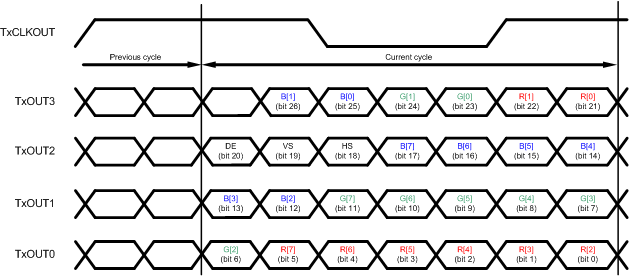 Figure 24. 24-bit Color FPD-Link (OpenLDI) Mapping: LSBs on TxOUT3 (MAPSEL=L)
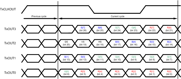 Figure 25. 24-bit Color FPD-Link (OpenLDI) Mapping: MSBs on TxOUT3 (MAPSEL=H)
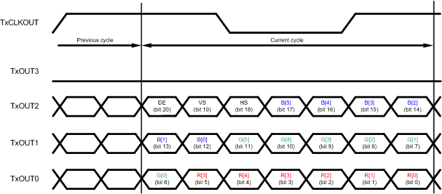 Figure 26. 18-bit Color FPD-Link (OpenLDI) Mapping (MAPSEL = L)
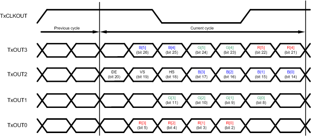 Figure 27. 18-bit Color FPD-Link (OpenLDI) Mapping (MAPSEL = H)
7.4.3 Low Frequency Optimization (LFMODE)
The LFMODE is set via register (Table 8) or by the LFMODE Pin. This mode optimizes device operation for lower input data clock ranges supported by the serializer. If LFMODE is Low (LFMODE=0, default), the TxCLKOUT± PCLK frequency is between 15 MHz and 96 MHz. If LFMODE is High (LFMODE=1), the TxCLKOUT± frequency is between 5 MHz and <15 MHz. Note: when the device LFMODE is changed, a PDB reset is required. When LFMODE is high (LFMODE=1), the line rate relative to the input data rate is multiplied by four. Thus, for the operating range of 5 MHz to <15 MHz, the line rate is 700 Mbps to <2.1 Gbps with an effective data payload of 175 Mbps to 525 Mbps. Note: for Backwards Compatibility Mode (BKWD=1), the line rate relative to the input data rate remains the same.
7.4.4 Mode Select (MODE_SEL)
Device configuration may be done via the MODE_SEL pin or via register (Table 7). A pullup resistor and a pulldown resistor of suggested values may be used to set the voltage ratio of the MODE_SEL input (VR4) and VDD33 to select one of the 9 possible selected modes. See Figure 28 and Table 6.
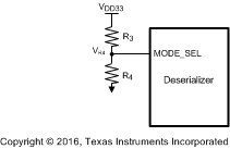 Figure 28. MODE_SEL Connection Diagram
Table 6. Configuration Select (MODE_SEL)
| NO. | Ideal Ratio (VR4/VDD33) | Ideal VR4 (V) | Suggested Resistor R3 (kΩ, 1% tol) | Suggested Resistor R4 (kΩ, 1% tol) | REPEAT | BKWD | I2S_B | LCBL |
|---|---|---|---|---|---|---|---|---|
| 1 | 0 | 0 | OPEN | 40.2 | L | L | L | L |
| 2 | 0.120 | 0.397 | 294 | 40.2 | L | L | H | L |
| 3 | 0.164 | 0.540 | 255 | 49.9 | H | L | L | L |
| 4 | 0.223 | 0.737 | 267 | 76.8 | H | L | H | L |
| 5 | 0.286 | 0.943 | 255 | 102 | L | L | L | H |
| 6 | 0.365 | 1.205 | 226 | 130 | L | L | H | H |
| 7 | 0.446 | 1.472 | 205 | 165 | H | L | L | H |
| 8 | 0.541 | 1.786 | 162 | 191 | H | L | H | H |
| 9 | 0.629 | 2.075 | 124 | 210 | L | H | L | L |
7.4.5 Repeater Configuration
The supported Repeater application provides a mechanism to extend transmission over multiple links to multiple display devices.
For the repeater application, this document refers to the DS90UB927Q-Q1 as the Transmitter (TX), and refers to the DS90UB924-Q1 as the Receiver (RX). Figure 29 shows the maximum configuration supported for Repeater implementations. Two levels of Repeaters are supported with a maximum of three Transmitters per Receiver.
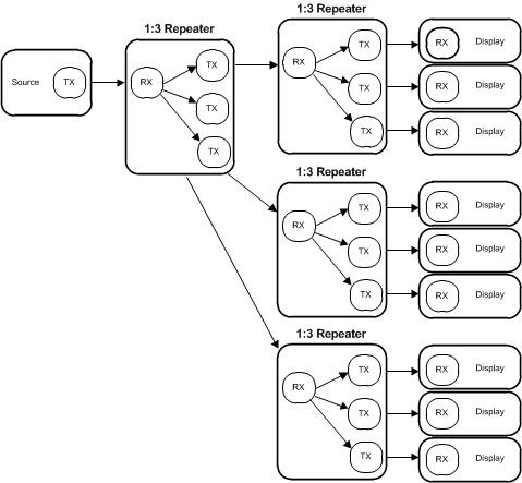 Figure 29. Maximum Repeater Application
In a repeater application, the I2C interface at each TX and RX is configured to transparently pass I2C communications upstream or downstream to any I2C device within the system. This includes a mechanism for assigning alternate IDs (Slave Aliases) to downstream devices in the case of duplicate addresses.
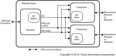 Figure 30. 1:2 Repeater Configuration
7.4.5.1 Repeater Connections
The Repeater requires the following connections between the Receiver and each Transmitter (Figure 31).
- Video Data – Connect all FPD-Link (OpenLDI) data and clock pairs
- I2C – Connect SCL and SDA signals. Both signals must be pulled up to VDD33 or VDDIO = 3.0 V to 3.6 V with 4.7-kΩ resistors.
- Audio (optional) – Connect I2S_CLK, I2S_WC, and I2S_Dx signals.
- IDx pin – Each Transmitter and Receiver must have an unique I2C address.
- REPEAT & MODE_SEL pins — All Transmitters and Receivers must be set into Repeater Mode.
- Interrupt pin – Connect DS90UB924-Q1 INTB_IN pin to the serializer INTB pin. The signal must be pulled up to VDDIO with a 10-kΩ resistor.
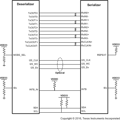 Figure 31. Repeater Connection Diagram
7.4.5.1.1 Repeater Fan-Out Electrical Requirements
Repeater applications requiring fan-out from one DS90UB924-Q1 deserializer to up to three DS90UB927Q-Q1 serializers requires special considerations for routing and termination of the FPD-Link (OpenLDI) differential traces. Figure 32 Details the requirements that must be met for each signal pair:
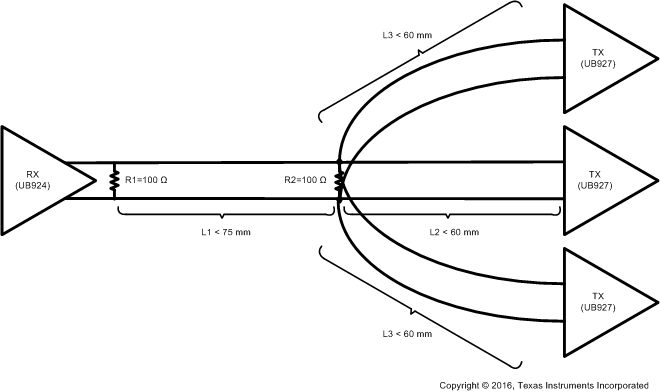 Figure 32. FPD-Link (OpenLDI) Fan-Out Electrical Requirements
7.5 Programming
The DS90UB924-Q1 may also be configured by the use of an I2C compatible serial control bus. Multiple devices may share the serial control bus (up to 10 device addresses supported). The device address is set via a resistor divider (R1 and R2 — see Figure 33) connected to the IDx pin.
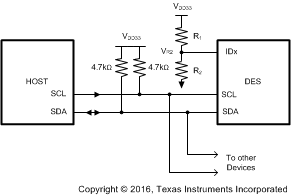 Figure 33. Serial Control Bus Connection
The serial control bus consists of two signals and an address configuration pin. SCL is a Serial Bus Clock Input/Output. SDA is the Serial Bus Data Input/Output signal. Both SCL and SDA signals require an external pullup resistor to VDD33 or VDDIO = 3.0 V to 3.6 V. For most applications, a 4.7-kΩ pullup resistor to VDD33 is recommended. The signals are either pulled HIGH, or driven LOW.
The IDx pin configures the control interface to one of 10 possible device addresses. A pullup resistor and a pulldown resistor is used to set the appropriate voltage ratio between the IDx input pin (VR2) and VDD33, each ratio corresponding to a specific device address. See Table 8.
Table 7. Serial Control Bus Addresses for IDx
| NO. | IDEAL RATIO VR2 / VDD33 |
IDEAL VR2
(V) |
SUGGESTED RESISTOR R1 kΩ (1% tol) | SUGGESTED RESISTOR R2 kΩ (1% tol) | ADDRESS 7'b | ADDRESS 8'b |
|---|---|---|---|---|---|---|
| 1 | 0 | 0 | OPEN | 40.2 or >10 | 0x2C | 0x58 |
| 2 | 0.995 | 0.302 | 226 | 97.6 | 0x33 | 0x66 |
| 3 | 1.137 | 0.345 | 215 | 113 | 0x34 | 0x68 |
| 4 | 1.282 | 0.388 | 200 | 127 | 0x35 | 0x6A |
| 5 | 1.413 | 0.428 | 187 | 140 | 0x36 | 0x6C |
| 6 | 1.570 | 0.476 | 174 | 158 | 0x37 | 0x6E |
| 7 | 1.707 | 0.517 | 154 | 165 | 0x38 | 0x70 |
| 8 | 1.848 | 0.560 | 150 | 191 | 0x39 | 0x72 |
| 9 | 1.997 | 0.605 | 137 | 210 | 0x3A | 0x74 |
| 10 | 2.535 | 0.768 | 90.9 | 301 | 0x3B | 0x76 |
The Serial Bus protocol is controlled by START, START-Repeated, and STOP phases. A START occurs when SCL transitions Low while SDA is High. A STOP occurs when SDA transitions High while SCL is also HIGH. See Figure 34.
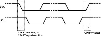 Figure 34. START and STOP Conditions
To communicate with a remote device, the host controller (master) sends the slave address and listens for a response from the slave. This response is referred to as an acknowledge bit (ACK). If a slave on the bus is addressed correctly, it Acknowledges (ACKs) the master by driving the SDA bus LOW. If the address doesn't match the slave address of device, it Not-acknowledges (NACKs) the master by letting SDA be pulled HIGH. ACKs also occur on the bus when data is being transmitted. When the master is writing data, the slave ACKs after every data byte is successfully received. When the master is reading data, the master ACKs after every data byte is received to let the slave know it wants to receive another data byte. When the master wants to stop reading, it NACKs after the last data byte and creates a stop condition on the bus. All communication on the bus begins with either a Start condition or a Repeated Start condition. All communication on the bus ends with a Stop condition. A READ is shown in Figure 35 and a WRITE is shown in Figure 36.
 Figure 35. Serial Control Bus — READ
 Figure 36. Serial Control Bus — WRITE
To support I2C transactions over the BCC. the I2C Master located at the DS90UB924-Q1 deserializer must support I2C clock stretching. For more information on I2C interface requirements and throughput considerations, refer to AN-2173 I2C Communication Over FPD-Link III with Bidirectional Control Channel SNLA131.
7.6 Register Maps
Table 8. Serial Control Bus Registers (1) (2)
| ADD (dec) |
ADD (hex) |
Register Name | Bit | Register Type |
Default (hex) |
Function | Description |
|---|---|---|---|---|---|---|---|
| 0 | 0x00 | I2C Device ID | 7:1 | RW | IDx | Device ID | 7–bit address of Deserializer Note: Read-only unless bit 0 is set |
| 0 | RW | ID Setting | I2C ID Setting 0: Device ID is from IDx pin 1: Register I2C Device ID overrides IDx pin |
||||
| 1 | 0x01 | Reset | 7:3 | 0x04 | Reserved | ||
| 2 | RW | BC Enable | Back Channel Enable 0: Disable 1: Enable |
||||
| 1 | RW | Digital RESET1 | Reset the entire digital block including registers This bit is self-clearing. 0: Normal operation (default) 1: Reset |
||||
| 0 | RW | Digital RESET0 | Reset the entire digital block except registers This bit is self-clearing 0: Normal operation (default) 1: Reset |
||||
| 2 | 0x02 | General Configuration 0 | 7 | RW | 0x00 | OEN | LVCMOS Output Enable. Self-clearing on loss of LOCK 0: Disable, Tristate Outputs (default) 1: Enable |
| 6 | RW | OEN/OSS_SEL Override | Output Enable and Output Sleep State Select override 0: Disable over-write (default) 1: Enable over-write |
||||
| 5 | RW | Auto Clock Enable | OSC Clock Output. Enable On loss of lock, OSC clock is output onto TxCLK± 0: Disable (default) 1: Enable |
||||
| 4 | RW | OSS_SEL | Output Sleep State Select. Enable Select to control output state during lock low period 0: Disable, Tri-State Outputs (default) 1: Enable |
||||
| 3 | RW | BKWD Override | Backwards Compatibility Mode Override 0: Use MODE_SEL pin (default) 1: Use register bit to set BKWD mode |
||||
| 2 | RW | BKWD Mode | Backwards Compatibility Mode Select 0: Backwards Compatibility Mode disabled (default) 1: Backwards Compatibility Mode enabled |
||||
| 1 | RW | LFMODE Override | Low Frequency Mode Override 0: Use LFMODE pin (default) 1: User register bit to set LFMODE |
||||
| 0 | RW | LFMODE | Low Frequency Mode 0: 15MHz ≤ PCLK ≤ 96MHz (default) 1: 5MHz ≤ PCLK < 15MHz |
||||
| 3 | 0x03 | General Configuration 1 | 7 | 0xF0 | Reserved | ||
| 6 | RW | Back channel CRC Generator Enable | Back Channel CRC Generator Enable 0: Disable 1: Enable (default) |
||||
| 5 | RW | Failsafe | Outputs Failsafe Mode. Determines the pull direction for undriven LVCMOS inputs 0: Pullup 1: Pulldown (default) |
||||
| 4 | RW | Filter Enable | HS, VS, DE two clock filter. When enabled, pulses less than two full PCLK cycles on the DE, HS, and VS inputs will be rejected 0: Filtering disable 1: Filtering enable (default) |
||||
| 3 | RW | I2C Pass-Through | I2C Pass-Through Mode Read/Write transactions matching any entry in the DeviceAlias registers will be passed through to the remote serializer I2C interface. 0: Pass-Through Disabled (default) 1: Pass-Through Enabled |
||||
| 2 | RW | Auto ACK | Automatically Acknowledge I2C transactions independent of the forward channel Lock state. 0: Disable (default) 1: Enable |
||||
| 1 | RW | DE Gate RGB | Gate RGB data with DE signal. RGB data is not gated with DE by default. However, to enable packetized audio in DS90UB924-Q1, this bit must be set. 0: Pass RGB data independent of DE in Backward Compatibility mode or interfacing to DS90UB925 or DS90UB927 1: Gate RGB data with DE in Backward Compatibility mode or interfacing to DS90UB925 or DS90UB927 |
||||
| 0 | Reserved | ||||||
| 4 | 0x04 | BCC Watchdog Control | 7:1 | RW | 0xFE | BCC Watchdog Timer | BCC Watchdog Timer The watchdog timer allows termination of a control channel transaction if it fails to complete within a programmed amount of time. This field sets the Bidirectional Control Channel Watchdog Timeout value in units of 2 milliseconds. This field must not be set to 0. |
| 0 | RW | BCC Watchdog Disable | Disable Bidirectional Control Channel Watchdog Timer 0: Enable (default) 1: Disable |
||||
| 5 | 0x05 | I2C Control 1 | 7 | RW | 0x1E | I2C Pass-All | I2C Pass-Through All Transactions. Pass all local I2C transactions to the remote serializer. 0: Disable (default) 1: Enable |
| 6:4 | RW | I2C SDA Hold | Internal I2C SDA Hold Time This field configures the amount of internal hold time is provided for the SDA input relative to the SCL input. Units are 50ns. |
||||
| 3:0 | RW | I2C Filter Depth | I2C Glitch Filter Depth This field configures the maximum width of glitch pulses on the SCL and SDA inputs that will be rejected. Units are 5 nanoseconds. |
||||
| 6 | 0x06 | I2C Control 2 | 7 | RW | 0x00 | Forward Channel Sequence Error | Control Channel Sequence Error Detected Indicates a sequence error has been detected in forward control channel. It this bit is set, an error may have occurred in the control channel operation. |
| 6 | RW | Clear Sequence Error | Clears the Sequence Error Detect bit This bit is not self-clearing. | ||||
| 5 | Reserved | ||||||
| 4:3 | RW | SDA Output Delay | SDA Output Delay This field configures output delay on the SDA output. Setting this value will increase output delay in units of 50ns. Nominal output delay values for SCL to SDA are: 00: 250ns (default) 01: 300ns 10: 350ns 11: 400ns |
||||
| 2 | RW | Local Write Disable | Disable Remote Writes to Local Registers through Serializer (Does not affect remote access to I2C slaves) 0: Remote write to local device registers (default) 1: Stop remote write to local device registers |
||||
| 1 | RW | I2C Bus Timer Speedup | Speed up I2C Bus Watchdog Timer 0: Timer expires after approximately 1s (default) 1: Timer expires after approximately 50µs |
||||
| 0 | RW | I2C Bus Timer Disable | Disable I2C Bus Watchdog Timer. When the I2C Watchdog Timer may be used to detect when the I2C bus is free or hung up following an invalid termination of a transaction. If SDA is high and no signaling occurs for approximately 1 second, the I2C bus is assumed to be free. If SDA is low and no signaling occurs, the device will attempt to clear the bus by driving 9 clocks on SCL |
||||
| 7 | 0x07 | Remote ID | 7:1 | R | 0x00 | Remote ID | Remote Serializer ID RW if bit 0 is set |
| 0 | RW | Freeze Device ID | Freeze Serializer Device ID 0: Auto-load Serializer Device ID (default) 1: Prevent auto-loading of Serializer Device ID from the remote device. The ID will be frozen at the value written. |
||||
| 8 | 0x08 | Slave ID[0] | 7:1 | RW | 0x00 | Slave Device ID0 | 7-bit Remote Slave Device ID 0 Configures the physical I2C address of the remote I2C Slave device attached to the remote Serializer. If an I2C transaction is addressed to the Slave Alias ID[0], the transaction will be re-mapped to this address before passing the transaction across the Bidirectional Control Channel to the Serializer. |
| 0 | Reserved | ||||||
| 9 | 0x09 | Slave ID[1] | 7:1 | RW | 0x00 | Slave Device ID1 | 7-bit Remote Slave Device ID1 Configures the physical I2C address of the remote I2C Slave device attached to the remote Serializer. If an I2C transaction is addressed to the Slave Alias ID[1], the transaction will be re-mapped to this address before passing the transaction across the Bidirectional Control Channel to the Serializer. |
| 0 | Reserved | ||||||
| 10 | 0x0A | Slave ID[2] | 7:1 | RW | 0x00 | Slave Device ID2 | 7-bit Remote Slave Device ID2 Configures the physical I2C address of the remote I2C Slave device attached to the remote Serializer. If an I2C transaction is addressed to the Slave Alias ID[2], the transaction will be re-mapped to this address before passing the transaction across the Bidirectional Control Channel to the Serializer. |
| 0 | Reserved | ||||||
| 11 | 0x0B | Slave ID[3] | 7:1 | RW | 0x00 | Slave Device ID3 | 7-bit Remote Slave Device ID3 Configures the physical I2C address of the remote I2C Slave device attached to the remote Serializer. If an I2C transaction is addressed to the Slave Alias ID[3], the transaction will be re-mapped to this address before passing the transaction across the Bidirectional Control Channel to the Serializer. |
| 0 | Reserved | ||||||
| 12 | 0x0C | Slave ID[4] | 7:1 | RW | 0x00 | Slave Device ID4 | 7-bit Remote Slave Device ID4 Configures the physical I2C address of the remote I2C Slave device attached to the remote Serializer. If an I2C transaction is addressed to the Slave Alias ID[4], the transaction will be re-mapped to this address before passing the transaction across the Bidirectional Control Channel to the Serializer. |
| 0 | Reserved | ||||||
| 13 | 0x0D | Slave ID[5] | 7:1 | RW | 0x00 | Slave Device ID5 | 7-bit Remote Slave Device ID5 Configures the physical I2C address of the remote I2C Slave device attached to the remote Serializer. If an I2C transaction is addressed to the Slave Alias ID[5], the transaction will be re-mapped to this address before passing the transaction across the Bidirectional Control Channel to the Serializer. |
| 0 | Reserved | ||||||
| 14 | 0x0E | Slave ID[6] | 7:1 | RW | 0x00 | Slave Device ID6 | 7-bit Remote Slave Device ID6 Configures the physical I2C address of the remote I2C Slave device attached to the remote Serializer. If an I2C transaction is addressed to the Slave Alias ID[6], the transaction will be re-mapped to this address before passing the transaction across the Bidirectional Control Channel to the Serializer. |
| 0 | Reserved | ||||||
| 15 | 0x0F | Slave ID[7] | 7:1 | RW | 0x00 | Slave Device ID7 | 7-bit Remote Slave Device ID 7 Configures the physical I2C address of the remote I2C Slave device attached to the remote Serializer. If an I2C transaction is addressed to the Slave Alias ID[7], the transaction will be re-mapped to this address before passing the transaction across the Bidirectional Control Channel to the Serializer. |
| 0 | Reserved | ||||||
| 16 | 0x10 | Slave Alias[0] | 7:1 | RW | 0x00 | Slave Device Alias 0 | 7-bit Remote Slave Alias 0 Configures the physical I2C address of the remote I2C Slave device attached to the remote Serializer. If an I2C transaction is addressed to the Slave Alias ID[0], the transaction will be re-mapped to the ID address before passing the transaction across the Bidirectional Control Channel to the Serializer. |
| 0 | Reserved | ||||||
| 17 | 0x11 | Slave Alias[1] | 7:1 | RW | 0x00 | Slave Device Alias 1 | 7-bit Remote Slave Alias 1 Configures the physical I2C address of the remote I2C Slave device attached to the remote Serializer. If an I2C transaction is addressed to the Slave Alias ID[1], the transaction will be re-mapped to the ID address before passing the transaction across the Bidirectional Control Channel to the Serializer. |
| 0 | Reserved | ||||||
| 18 | 0x12 | Slave Alias[2] | 7:1 | RW | 0x00 | Slave Device Alias 2 | 7-bit Remote Slave Alias 2 Configures the physical I2C address of the remote I2C Slave device attached to the remote Serializer. If an I2C transaction is addressed to the Slave Alias ID[2], the transaction will be re-mapped to the ID address before passing the transaction across the Bidirectional Control Channel to the Serializer. |
| 0 | Reserved | ||||||
| 19 | 0x13 | Slave Alias[3] | 7:1 | RW | 0x00 | Slave Device Alias 3 | 7-bit Remote Slave Alias 3 Configures the physical I2C address of the remote I2C Slave device attached to the remote Serializer. If an I2C transaction is addressed to the Slave Alias ID[3], the transaction will be re-mapped to the ID address before passing the transaction across the Bidirectional Control Channel to the Serializer. |
| 0 | Reserved | ||||||
| 20 | 0x14 | Slave Alias[4] | 7:1 | RW | 0x00 | Slave Device Alias 4 | 7-bit Remote Slave Alias 4 Configures the physical I2C address of the remote I2C Slave device attached to the remote Serializer. If an I2C transaction is addressed to the Slave Alias ID[4], the transaction will be re-mapped to the ID address before passing the transaction across the Bidirectional Control Channel to the Serializer. |
| 0 | Reserved | ||||||
| 21 | 0x15 | Slave Alias[5] | 7:1 | RW | 0x00 | Slave Device Alias 5 | 7-bit Remote Slave Alias 5 Configures the physical I2C address of the remote I2C Slave device attached to the remote Serializer. If an I2C transaction is addressed to the Slave Alias ID[5], the transaction will be re-mapped to the ID address before passing the transaction across the Bidirectional Control Channel to the Serializer. |
| 0 | Reserved | ||||||
| 22 | 0x16 | Slave Alias[6] | 7:1 | RW | 0x00 | Slave Device Alias 6 | 7-bit Remote Slave Alias 6 Configures the physical I2C address of the remote I2C Slave device attached to the remote Serializer. If an I2C transaction is addressed to the Slave Alias ID[6], the transaction will be re-mapped to the ID address before passing the transaction across the Bidirectional Control Channel to the Serializer. |
| 0 | Reserved | ||||||
| 23 | 0x17 | Slave Alias[7] | 7:1 | RW | 0x00 | Slave Device Alias 7 | 7-bit Remote Slave Alias 7 Configures the physical I2C address of the remote I2C Slave device attached to the remote Serializer. If an I2C transaction is addressed to the Slave Alias ID[7], the transaction will be re-mapped to the ID address before passing the transaction across the Bidirectional Control Channel to the Serializer. |
| 0 | Reserved | ||||||
| 24 | 0x18 | Mailbox[0] | 7:0 | RW | 0x00 | Mailbox Register 0 | Mailbox Register 0 This register may be used to temporarily store temporary data, such as status or multi-master arbitration |
| 25 | 0x19 | Mailbox[1] | 7:0 | RW | 0x01 | Mailbox Register 1 | Mailbox Register 1 This register may be used to temporarily store temporary data, such as status or multi-master arbitration |
| 27 | 0x1B | Frequency Counter | 7:0 | RW | 0x00 | Frequency Count | Frequency Counter control A write to this register will enable a frequency counter to count the number of pixel clock during a specified time interval. The time interval is equal to the value written multiplied by the oscillator clock period (nominally 50ns). A read of the register returns the number of pixel clock edges seen during the enabled interval. The frequency counter will saturate at 0xff if it reaches the maximum value. The frequency counter will provide a rough estimate of the pixel clock period. If the pixel clock frequency is known, the frequency counter may be used to determine the actual oscillator clock frequency. |
| 28 | 0x1C | General Status | 7:4 | 0x00 | Reserved | ||
| 3 | R | I2S Locked | I2S Lock Status 0: I2S PLL controller not locked (default) 1: I2S PLL controller locked to input I2S clock |
||||
| 2 | R | CRC Error | CRC Error Detected 0: No CRC errors detected 1: CRC errors detected |
||||
| 1 | Reserved | ||||||
| 0 | R | LOCK | Deserializer CDR and PLL Locked to recovered clock frequency 0: Deserializer not Locked (default) 1: Deserializer Locked to recovered clock |
||||
| 29 | 0x1D | GPIO0 Configuration | 7:4 | R | 0x20 | Revision ID | Device Revision ID: 0010: Production Device |
| 3 | RW | GPIO0 Output Value | Local GPIO Output Value This value is output on the GPIO pin when the GPIO function is enabled, the local GPIO direction is Output, and remote GPIO control is disabled. 0: Output LOW (default) 1: Output HIGH |
||||
| 2 | RW | GPIO0 Remote Enable | Remote GPIO Control 0: Disable GPIO control from remote device (default) 1: Enable GPIO control from remote device. The GPIO pin will be an output, and the value is received from the remote device. |
||||
| 1 | RW | GPIO0 Direction | Local GPIO Direction 0: Output (default) 1: Input |
||||
| 0 | RW | GPIO0 Enable | GPIO Function Enable 0: Enable normal operation (default) 1: Enable GPIO operation |
||||
| 30 | 0x1E | GPIO1 and GPIO2 Configuration | 7 | RW | 0x00 | GPIO2 Output Value | Local GPIO Output Value This value is output on the GPIO pin when the GPIO function is enabled, the local GPIO direction is Output, and remote GPIO control is disabled. 0: Output LOW (default) 1: Output HIGH |
| 6 | RW | GPIO2 Remote Enable | Remote GPIO Control 0: Disable GPIO control from remote device (default) 1: Enable GPIO control from remote device. The GPIO pin will be an output, and the value is received from the remote device. |
||||
| 5 | RW | GPIO2 Direction | Local GPIO Direction 0: Output (default) 1: Input |
||||
| 4 | RW | GPIO2 Enable | GPIO Function Enable 0: Enable normal operation (default) 1: Enable GPIO operation |
||||
| 3 | RW | GPIO1 Output Value | Local GPIO Output Value This value is output on the GPIO pin when the GPIO function is enabled, the local GPIO direction is Output, and remote GPIO control is disabled. 0: Output LOW (default) 1: Output HIGH |
||||
| 2 | RW | GPIO1 Remote Enable | Remote GPIO Control 0: Disable GPIO control from remote device (default) 1: Enable GPIO control from remote device. The GPIO pin will be an output, and the value is received from the remote device. |
||||
| 1 | RW | GPIO1 Direction | Local GPIO Direction 1: Input 0: Output |
||||
| 0 | RW | GPIO1 Enable | GPIO function enable 1: Enable GPIO operation 0: Enable normal operation |
||||
| 31 | 0x1F | GPIO3 Configuration | 7:4 | 0x00 | Reserved | ||
| 3 | RW | GPIO3 Output Value | Local GPIO Output Value This value is output on the GPIO pin when the GPIO function is enabled, the local GPIO direction is Output, and remote GPIO control is disabled. 0: Output LOW (default) 1: Output HIGH |
||||
| 2 | RW | GPIO3 Remote Enable | Remote GPIO Control 0: Disable GPIO control from remote device (default) 1: Enable GPIO control from remote device. The GPIO pin will be an output, and the value is received from the remote device. |
||||
| 1 | RW | GPIO3 Direction | Local GPIO Direction 0: Output (default) 1: Input |
||||
| 0 | RW | GPIO3 Enable | GPIO Function Enable 0: Enable normal operation (default) 1: Enable GPIO operation |
||||
| 32 | 0x20 | GPIO_REG5 and GPIO_REG6 Configuration | 7 | RW | 0x00 | GPIO_REG6 Output Value | Local GPIO Output Value This value is output on the GPIO pin when the GPIO function is enabled, and the local GPIO direction is Output. 0: Output LOW (default) 1: Output HIGH |
| 6 | Reserved | ||||||
| 5 | RW | GPIO_REG6 Direction | Local GPIO Direction 0: Output (default) 1: Input |
||||
| 4 | RW | GPIO_REG6 Enable | GPIO Function Enable 0: Enable normal operation (default) 1: Enable GPIO operation |
||||
| 3 | RW | GPIO_REG5 Output Value | Local GPIO Output Value This value is output on the GPIO pin when the GPIO function is enabled, and the local GPIO direction is Output. 0: Output LOW (default) 1: Output HIGH |
||||
| 2 | Reserved | ||||||
| 1 | RW | GPIO_REG5 Direction | Local GPIO Direction 0: Output (default) 1: Input |
||||
| 0 | RW | GPIO_REG5 Enable | GPIO Function Enable 0: Enable normal operation (default) 1: Enable GPIO operation |
||||
| 33 | 0x21 | GPIO_REG7 and GPIO_REG8 Configuration | 7 | RW | 0x00 | GPIO_REG8 Output Value | Local GPIO Output Value This value is output on the GPIO pin when the GPIO function is enabled, and the local GPIO direction is Output. 0: Output LOW (default) 1: Output HIGH |
| 6 | Reserved | ||||||
| 5 | RW | GPIO_REG8 Direction | Local GPIO Direction 0: Output (default) 1: Input |
||||
| 4 | RW | GPIO_REG8 Enable | GPIO Function Enable 0: Enable normal operation (default) 1: Enable GPIO operation |
||||
| 3 | RW | GPIO_REG7 Output Value | Local GPIO Output Value This value is output on the GPIO pin when the GPIO function is enabled, and the local GPIO direction is Output. 0: Output LOW (default) 1: Output HIGH |
||||
| 2 | Reserved | ||||||
| 1 | RW | GPIO_REG7 Direction | Local GPIO Direction 0: Output (default) 1: Input |
||||
| 0 | RW | GPO_REG7 Enable | GPIO Function Enable 0: Enable normal operation (default) 1: Enable GPIO operation |
||||
| 34 | 0x22 | Data Path Control | 7 | RW | 0x00 | Override FC Configuration | Override Configuration Loaded by Forward Channel 0: Allow forward channel loading of this register (default) 1: Disable loading of this register from the forward channel, keeping locally written values intact Bits [6:0] are RW if this bit is set |
| 6 | Reserved | ||||||
| 5 | RW | DE Polarity | This bit indicates the polarity of the DE (Data Enable) signal. 0: DE is positive (active high, idle low) (default) 1: DE is inverted (active low, idle high) |
||||
| 4 | RW | I2S Repeater Regen | Regenerate I2S Data From Repeater I2S Pins 0: Output packetized audio on RGB video output pins. (default) 1: Do not output packaged audio data on RGB video output pins. |
||||
| 3 | RW | I2S Channel B Enable Override | I2S Channel B Override 0: Set I2S Channel B Disabled (default) 1: Set I2S Channel B Enable from register |
||||
| 2 | RW | 18-bit Video Select | Video Color Depth Mode 0: Select 24-bit video mode (default) 1: Select 18-bit video mode |
||||
| 1 | RW | I2S Transport Select | Select I2S Transport Mode 0: Enable I2S Data Island Transport (default) 1: Enable I2S Data Forward Channel Frame Transport |
||||
| 0 | RW | I2S Channel B Enable | I2S Channel B Enable 0: I2S Channel B disabled (default) 1: Enable I2S Channel B |
||||
| 35 | 0x23 | Rx Mode Status | 7 | 0x10 | Reserved | ||
| 6:4 | Reserved | ||||||
| 3 | RW | LFMODE Status | Low Frequency Mode (LFMODE) pin status 0: 15 ≤ TxCLKOUT ≤ 96MHz (default) 1: 5 ≤ TxCLKOUT < 15MHz |
||||
| 2 | RW | REPEAT Status | Repeater Mode (REPEAT) pin Status 0: Non-repeater (default) 1: Repeater |
||||
| 1 | RW | BKWD Status | Backward Compatible Mode (BKWD) Status 0: Compatible to DS90UB925/7Q (default) 1: Backward compatible to DS90UR905/7Q |
||||
| 0 | RW | I2S Channel B Status | I2S Channel B Mode (I2S_DB) Status 0: I2S_DB inactive (default) 1: I2S_DB active |
||||
| 36 | 0x24 | BIST Control | 7:4 | 0x08 | Reserved | ||
| 3 | RW | BIST Pin Config | BIST Pin Configuration 0: BIST enabled from register 1: BIST enabled from pin (default) |
||||
| 2:1 | RW | OSC Clock Source | Internal OSC clock select for Functional Mode or BIST. Functional Mode when PCLK is not present and 0x03[1]=1. 00: 33 MHz Oscillator (default) 01: 33 MHz Oscillator Note: In LFMODE=1, the internal oscillator is 12.5MHz |
||||
| 0 | RW | BIST Enable | BIST Control 0: Disabled (default) 1: Enabled |
||||
| 37 | 0x25 | BIST Error | 7:0 | R | 0x00 | BIST Error Count | Errors Detected During BIST Records the number (up to 255) of forward-channel errors detected during BIST. The value stored in this register is only valid after BIST terminates (BISTEN = 0). Resets on PDB = 0 or start of another BIST (BISTEN = 1). |
| 38 | 0x26 | SCL High Time | 7:0 | RW | 0x83 | SCL High Time | I2C Master SCL High Time This field configures the high pulse width of the SCL output when the deserializer is the Master on the local I2C bus. Units are 50 ns for the nominal oscillator clock frequency. |
| 39 | 0x27 | SCL Low Time | 7:0 | RW | 0x84 | SCL Low Time | I2C SCL Low Time This field configures the low pulse width of the SCL output when the deserializer is the Master on the local I2C bus. This value is also used as the SDA setup time by the I2C Slave for providing data prior to releasing SCL during accesses over the Bidirectional Control Channel. Units are 50 ns for the nominal oscillator clock frequency. |
| 40 | 0x28 | Data Path Control 2 | 7 | RW | 0x00 | Block I2S Auto Config | Override Forward Channel Configuration 0: Enable forward-channel loading of this register 1: Disable loading of this register from the forward channel, keeping local values intact |
| 6:4 | Reserved | ||||||
| 3 | RW | Aux I2S Enable | Auxiliary I2S Channel Enable 0: Normal GPIO[1:0] operation 1: Enable Aux I2S channel on GPIO1 (AUX word select) and GPIO0 (AUX data) |
||||
| 2 | RW | I2S Disable | Disable All I2S Outputs 0: I2S Outputs Enabled (default) 1: I2S Outputs Disabled |
||||
| 1 | Reserved | ||||||
| 0 | RW | I2S Surround | Enable 5.1- or 7.1-channel I2S audio transport 0: 2-channel or 4-channel I2S audio is enabled as configured in register or MODE_SEL (default) 1: 5.1- or 7.1-channel audio is enabled Note that I2S Data Island Transport is the only option for surround audio. Also note that in a repeater, this bit may be overridden by the in-band I2S mode detection. |
||||
| 41 | 0x29 | FRC Control | 7 | RW | 0x00 | Timing Mode Select | Select Display Timing Mode 0: DE only Mode (default) 1: Sync Mode (VS,HS) |
| 6 | RW | HS Polarity | Horizontal Sync Polarity Select 0: Active High (default) 1: Active Low |
||||
| 5 | RW | VS Polarity | Vertical Sync Polarity Select 0: Active High (default) 1: Active Low |
||||
| 4 | RW | DE Polarity | Data Enable Sync Polarity Select 0: Active High (default) 1: Active Low |
||||
| 3 | RW | FRC2 Enable | FRC2 Enable 0: FRC2 disable (default) 1: FRC2 enable |
||||
| 2 | RW | FRC1 Enable | FRC1 Enable 0: FRC1 disable (default) 1: FRC1 enable |
||||
| 1 | RW | Hi-FRC2 Enable | Hi-FRC2 Enable 0: Hi-FRC2 enable (default) 1: Hi-FRC2 disable |
||||
| 0 | RW | Hi-FRC1 Enable | Hi-FRC1 Enable 0: Hi-FRC1 enable (default) 1: Hi-FRC1 disable |
||||
| 43 | 0x2B | I2S Control | 7 | RW | 0x00 | I2S PLL Override | Override I2S PLL 0: PLL override disabled (default) 1: PLL override enabled |
| 6 | RW | I2S PLL Enable | Enable I2S PLL 0: I2S PLL is on for I2S data jitter cleaning (default) 1: I2S PLL is off. No jitter cleaning |
||||
| 5:1 | Reserved | ||||||
| 0 | RW | I2S Clock Edge | I2S Clock Edge Select 0: I2S Data is strobed on the Falling Clock Edge (default) 1: I2S Data is strobed on the Rising Clock Edge |
||||
| 53 | 0x35 | AEQ Control | 7 | 0x00 | Reserved | ||
| 6 | RW | AEQ Restart | Restart AEQ adaptation from initial (Floor) values 0: Normal operation (default) 1: Restart AEQ adaptation Note: This bit is not self-clearing. It must be set, then reset. |
||||
| 5 | RW | LCBL Override | Override LCBL Mode Set by MODE_SEL 0: LCBL controlled by MODE_SEL pin 1: LCBL controlled by register |
||||
| 4 | RW | LCBL | Set LCBL Mode 0: LCBL Mode disabled 1: LCBL Mode enabled. AEQ Floor value is controlled from Adaptive EQ MIN/MAX register |
||||
| 3:0 | Reserved | ||||||
| 57 | 0x39 | PG Internal Clock Enable | 7:2 | 0x00 | Reserved | ||
| 1 | RW | PG INT CLK | Enable Pattern Generator Internal Clock This bit must be set to use the Pattern Generator Internal Clock Generation 0: Pattern Generator with external PCLK 1: Pattern Generator with internal PCLK See TI Application Note AN-2198 for details |
||||
| 0 | Reserved | ||||||
| 58 | 0x3A | I2S DIVSEL | 7 | RW | 0x00 | MCLK Div Override | Override MCLK Divider Setting 0: No override for MCLK divider (default) 1: Override divider select for MCLK |
| 6:4 | RW | MCLK Div | See Table 4 | ||||
| 3:0 | Reserved | ||||||
| 59 | 0x3B | Adaptive EQ Status | 7:6 | R | Reserved | ||
| 5:0 | R | EQ Status | Equalizer Status Current equalizer level set by AEQ or Override Register |
||||
| 65 | 0x41 | Link Error Count | 7:5 | 0x03 | Reserved | ||
| 4 | RW | Link Error Count Enable | Enable serial link data integrity error count. 1: Enable error count 0: Disable |
||||
| 3:0 | RW | Link Error Count | Link error count threshold. Counter is pixel clock based. CLK0, CLK1, and DCA are monitored for link errors. If error count is enabled, Deserializer will lose lock once error count reaches threshold. If disabled, Deserializer will lose lock with one error. Video, audio, GPIO, and I2C data bits are not checked for errors. | ||||
| 68 | 0x44 | Adaptive Equalizer Bypass | 7:5 | RW | 0x60 | EQ Stage 1 Select Value | EQ Stage 1 select value. Used if adaptive EQ is bypassed. Used if adaptive EQ is bypassed. |
| 4 | Reserved | ||||||
| 3:1 | RW | EQ Stage 2 Select Value | EQ Stage 2 select value. Used if adaptive EQ is bypassed Used if adaptive EQ is bypassed. | ||||
| 0 | RW | Adaptive EQ Bypass | Bypass Adaptive EQ Overrides Adaptive EQ search and sets the EQ to the static value configured in this register 0: Enable adaptive EQ (default) 1: Disable adaptive EQ (to write EQ select values) |
||||
| 69 | 0x45 | Adaptive EQ MIN/MAX | 7:4 | RW | 0x88 | Reserved | |
| 3:0 | RW | Adaptive EQ Floor | Adaptive Equalizer Floor Value Sets the AEQ floor value when Long Cable Mode (LCBL) is enabled by register or MODE_SEL |
||||
| 73 | 0x49 | Map Select | 7 | R | 0x00 | MAPSEL Pin Status | Returns Status of MAPSEL pin |
| 6 | RW | MAPSEL Override | Map Select (MAPSEL) Setting Override 0: MAPSEL set from pin 1: MAPSEL set from register |
||||
| 5 | RW | MAPSEL | Map Select (MAPSEL) Setting 0: LSBs on TxOUT3± 1: MSBs on TxOUT3± |
||||
| 4:0 | Reserved | ||||||
| 75 | 0x4B | LVDS Driver Setting | 7:2 | 0x08 | Reserved | ||
| 1:0 | RW | LVDS VOD Control | 00: 400mV differential (default) 01: 600mV differential |
||||
| 86 | 0x56 | Loop-Through Driver | 7:4 | 0x08 | Reserved | ||
| 3 | RW | Loop-Through Driver Enable | Enable CML Loop-Through Driver (CMLOUTP/CMLOUTN) 0: Enable 1: Disable (default) |
||||
| 2:0 | Reserved | ||||||
| 100 | 0x64 | Pattern Generator Control | 7:4 | RW | 0x10 | Pattern Generator Select | Fixed Pattern Select Selects the pattern to output when in Fixed Pattern Mode. Scaled patterns are evenly distributed across the horizontal or vertical active regions. This field is ignored when Auto-Scrolling Mode is enabled. xxxx: normal/inverted 0000: Checkerboard 0001: White/Black (default) 0010: Black/White 0011: Red/Cyan 0100: Green/Magenta 0101: Blue/Yellow 0110: Horizontal Black-White/White-Black 0111: Horizontal Black-Red/White-Cyan 1000: Horizontal Black-Green/White-Magenta 1001: Horizontal Black-Blue/White-Yellow 1010: Vertical Black-White/White— Black 1011: Vertically Scaled Black to Red/White to Cyan 1100: Vertical Black-Green/White-Magenta 1101: Vertical Black-Blue/White-Yellow 1110: Custom color (or its inversion) configured in PGRS, PGGS, PGBS registers 1111: VCOM See TI App Note AN-2198 |
| 3 | Reserved | ||||||
| 2 | RW | Color Bars Pattern | Enable Color Bars Pattern 0: Color Bars disabled (default) 1: Color Bars enabled Overrides the selection from bits [7:4] |
||||
| 1 | RW | VCOM Pattern Reverse | Reverse order of color bands in VCOM pattern 0: Color sequence from top left is (YCBR) (default) 1: Color sequence from top left is (RBCY) |
||||
| 0 | RW | Pattern Generator Enable | Pattern Generator Enable 0: Disable Pattern Generator (default) 1: Enable Pattern Generator See TI App Note AN-2198 |
||||
| 101 | 0x65 | Pattern Generator Configuration | 7 | 0x00 | Reserved | ||
| 6 | RW | Checkerboard Scale | Scale Checkerboard Patterns: 0: Normal operation (each square is 1x1 pixel) (default) 1: Scale checkered patterns (VCOM and checkerboard) by 8 (each square is 8x8 pixels) Setting this bit gives better visibility of the checkered patterns. |
||||
| 5 | RW | Custom Checkerboard | Use Custom Checkerboard Color 0: Use white and black in the Checkerboard pattern (default) 1: Use the Custom Color and black in the Checkerboard pattern |
||||
| 4 | RW | PG 18–bit Mode | 18-bit Mode Select: 0: Enable 24-bit pattern generation. Scaled patterns use 256 levels of brightness. (default) 1: Enable 18-bit color pattern generation. Scaled patterns will have 64 levels of brightness and the R, G, and B outputs use the six most significant color bits. |
||||
| 3 | RW | External Clock | Select External Clock Source: 0: Selects the internal divided clock when using internal timing (default) 1: Selects the external pixel clock when using internal timing. This bit has no effect in external timing mode (PATGEN_TSEL = 0). |
||||
| 2 | RW | Timing Select | Timing Select Control: 0: the Pattern Generator uses external video timing from the pixel clock, Data Enable, Horizontal Sync, and Vertical Sync signals. (default) 1: The Pattern Generator creates its own video timing as configured in the Pattern Generator Total Frame Size, Active Frame Size. Horizontal Sync Width, Vertical Sync Width, Horizontal Back Porch, Vertical Back Porch, and Sync Configuration registers. |
||||
| 1 | RW | Color Invert | Enable Inverted Color Patterns: 0: Do not invert the color output. (default) 1: Invert the color output. |
||||
| 0 | RW | Auto Scroll | Auto Scroll Enable: 0: The Pattern Generator retains the current pattern. (default) 1: The Pattern Generator will automatically move to the next enabled pattern after the number of frames specified in the Pattern Generator Frame Time (PGFT) register. See TI App Note AN-2198 |
||||
| 102 | 0x66 | PGIA | 7:0 | RW | 0x00 | PG Indirect Address | This 8-bit field sets the indirect address for accesses to indirectly-mapped registers. It must be written prior to reading or writing the Pattern Generator Indirect Data register. See TI App Note AN-2198 |
| 103 | 0x67 | PGID | 7:0 | RW | 0x00 | PG Indirect Data | When writing to indirect registers, this register contains the data to be written. When reading from indirect registers, this register contains the read back value. See TI App Note AN-2198 AN-2198 |
| 110 | 0x6E | GPI Pin Status 1 | 7 | R | 0x00 | GPI7 Pin Status | GPI7 Pin Status. Readable when REG_GPIO7 is set as an input. |
| 6 | R | GPI6 Pin Status | GPI6 Pin Status. Readable when REG_GPIO6 is set as an input. | ||||
| 5 | R | GPI5 Pin Status | GPI5 Pin Status. Readable when REG_GPIO5 is set as an input. | ||||
| 4 | Reserved | ||||||
| 3 | R | GPI3 Pin Status | GPI3 Pin Status. Readable when GPIO3 is set as an input. | ||||
| 2 | R | GPI2 Pin Status | GPI2 Pin Status. Readable when GPIO2 is set as an input. | ||||
| 1 | R | GPI1 Pin Status | GPI1 Pin Status. Readable when GPIO1 is set as an input. | ||||
| 0 | R | GPI0 Pin Status | GPI0 Pin Status. Readable when GPIO0 is set as an input. | ||||
| 111 | 0x6F | GPI Pin Status 2 | 7:1 | 0x00 | Reserved | ||
| 0 | R | GPI8 Pin Status | GPI8 Pin Status. Readable when REG_GPIO8 is set as an input. |