ZHCSD38B November 2014 – August 2019 DS90UB929-Q1
PRODUCTION DATA.
- 1 特性
- 2 应用
- 3 说明
- 4 修订历史记录
- 5 Pin Configuration and Functions
-
6 Specifications
- 6.1 Absolute Maximum Ratings
- 6.2 ESD Ratings
- 6.3 Recommended Operating Conditions
- 6.4 Thermal Information
- 6.5 DC Electrical Characteristics
- 6.6 AC Electrical Characteristics
- 6.7 DC And AC Serial Control Bus Characteristics
- 6.8 Recommended Timing for the Serial Control Bus
- 6.9 Timing Diagrams
- 6.10 Typical Characteristics
-
7 Detailed Description
- 7.1 Overview
- 7.2 Functional Block Diagram
- 7.3
Feature Description
- 7.3.1 High-Definition Multimedia Interface (HDMI)
- 7.3.2 Transition Minimized Differential Signaling
- 7.3.3 Enhanced Display Data Channel
- 7.3.4 Extended Display Identification Data (EDID)
- 7.3.5 Consumer Electronics Control (CEC)
- 7.3.6 +5-V Power Signal
- 7.3.7 Hot Plug Detect (HPD)
- 7.3.8 High-Speed Forward Channel Data Transfer
- 7.3.9 Back Channel Data Transfer
- 7.3.10 Power Down (PDB)
- 7.3.11 Serial Link Fault Detect
- 7.3.12 Interrupt Pin (INTB)
- 7.3.13 Remote Interrupt Pin (REM_INTB)
- 7.3.14 General-Purpose I/O
- 7.3.15 Backward Compatibility
- 7.3.16 Audio Modes
- 7.3.17 Built-In Self Test (BIST)
- 7.3.18 Internal Pattern Generation
- 7.3.19 Spread Spectrum Clock Tolerance
- 7.4 Device Functional Modes
- 7.5
Programming
- 7.5.1 Serial Control Bus
- 7.5.2 Multi-Master Arbitration Support
- 7.5.3 I2C Restrictions on Multi-Master Operation
- 7.5.4 Multi-Master Access to Device Registers for Newer FPD-Link III Devices
- 7.5.5 Multi-Master Access to Device Registers for Older FPD-Link III Devices
- 7.5.6 Restrictions on Control Channel Direction for Multi-Master Operation
- 7.6 Register Maps
- 8 Application and Implementation
- 9 Power Supply Recommendations
- 10Layout
- 11器件和文档支持
- 12机械、封装和可订购信息
7.3.17.1 BIST Configuration And Status
The BIST mode is enabled at the deserializer by pin (BISTEN) or BIST configuration register. The test may select either an external TMDS clock or the internal Oscillator clock (OSC) frequency. In the absence of the TMDS clock, the user can select the internal OSC frequency at the deserializer through the BISTC pin or BIST configuration register.
When BIST is activated at the deserializer, a BIST enable signal is sent to the serializer through the Back Channel. The serializer outputs a test pattern and drives the link at speed. The deserializer detects the test pattern and monitors it for errors. The deserializer PASS output pin toggles to flag each frame received containing one or more errors. The serializer also tracks errors indicated by the CRC fields in each back channel frame.
The BIST status can be monitored in real time on the deserializer PASS pin with each detected error resulting in a half-pixel clock period toggled LOW. After BIST is deactivated, the result of the last test is held on the PASS output until reset (new BIST test or Power Down). A High on PASS indicates no errors were detected. A Low on PASS indicates one or more errors were detected. The duration of the test is controlled by the pulse width applied to the deserializer BISTEN pin. LOCK is valid throughout the entire duration of BIST.
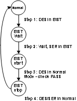
See Figure 14 for the BIST mode flow diagram.
Step 1: The Serializer is paired with another FPD-Link III Deserializer, then BIST Mode is enabled through the BISTEN pin or through register on the Deserializer. Right after BIST is enabled, part of the BIST sequence requires bit 0x04[5] be toggled locally on the Serializer (set 0x04[5]=1, then set 0x04[5]=0). The desired clock source is selected through the deserializer BISTC pin or through register on the Deserializer.
Step 2: An all-zeros pattern is balanced, scrambled, randomized, and sent through the FPD-Link III interface to the deserializer. When the serializer and the deserializer are in BIST mode and the deserializer acquires Lock, the PASS pin of the deserializer goes high and BIST starts checking the data stream. If an error in the payload (1 to 35) is detected, the PASS pin will switch low for one-half of the clock period. During the BIST test, the PASS output can be monitored and counted to determine the payload error rate.
Step 3: To stop the BIST mode, the deserializer BISTEN pin is set low. The deserializer stops checking the data. The final test result is held on the PASS pin. If the test ran error-free, the PASS output will remain HIGH. If there one or more errors were detected, the PASS output will output constant LOW. The PASS output state is held until a new BIST is run, the device is reset, or the device is powered down. The BIST duration is user-controlled by the duration of the BISTEN signal.
Step 4: The link returns to normal operation after the deserializer BISTEN pin is low. Figure 15 shows the waveform diagram of a typical BIST test for two cases. Case 1 is error-free, and Case 2 shows one with multiple errors. In most cases, it is difficult to generate errors due to the robustness of the link (differential data transmission and so forth), thus they may be introduced by greatly extending the cable length, faulting the interconnect medium, or reducing signal condition enhancements (Rx Equalization).
For more information on using BIST, refer to the white paper: Using BIST on 94x.
 Figure 14. BIST Mode Flow Diagram