ZHCSD36A November 2014 – March 2019 DS90UB947-Q1
PRODUCTION DATA.
- 1 特性
- 2 应用
- 3 说明
- 4 修订历史记录
- 5 Pin Configuration and Functions
-
6 Specifications
- 6.1 Absolute Maximum Ratings
- 6.2 ESD Ratings
- 6.3 Recommended Operating Conditions
- 6.4 Thermal Information
- 6.5 DC Electrical Characteristics
- 6.6 AC Electrical Characteristics
- 6.7 DC and AC Serial Control Bus Characteristics
- 6.8 Recommended Timing for the Serial Control Bus
- 6.9 Timing Diagrams
- 6.10 Typical Characteristics
-
7 Detailed Description
- 7.1 Overview
- 7.2 Functional Block Diagram
- 7.3
Feature Description
- 7.3.1 High-Speed Forward Channel Data Transfer
- 7.3.2 Back Channel Data Transfer
- 7.3.3 FPD-Link III Port Register Access
- 7.3.4 OpenLDI Input Frame and Color Bit Mapping Select
- 7.3.5 Video Control Signals
- 7.3.6 Power Down (PDB)
- 7.3.7 Serial Link Fault Detect
- 7.3.8 Interrupt Pin (INTB)
- 7.3.9 Remote Interrupt Pin (REM_INTB)
- 7.3.10 General-Purpose I/O
- 7.3.11 SPI Communication
- 7.3.12 Backward Compatibility
- 7.3.13 Audio Modes
- 7.3.14 Repeater
- 7.3.15 Built-In Self Test (BIST)
- 7.3.16 Internal Pattern Generation
- 7.4 Device Functional Modes
- 7.5
Programming
- 7.5.1 Serial Control Bus
- 7.5.2 Multi-Master Arbitration Support
- 7.5.3 I2C Restrictions on Multi-Master Operation
- 7.5.4 Multi-Master Access to Device Registers for Newer FPD-Link III Devices
- 7.5.5 Multi-Master Access to Device Registers for Older FPD-Link III Devices
- 7.5.6 Restrictions on Control Channel Direction for Multi-Master Operation
- 7.6 Register Maps
- 8 Application and Implementation
- 9 Power Supply Recommendations
- 10Layout
- 11器件和文档支持
- 12机械、封装和可订购信息
7.3.14.1 Repeater Configuration
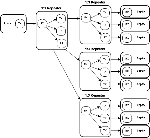
In the repeater application, this document refers to the DS90UB947-Q1 Serializer or as the Transmitter (TX), and refers to the DS90UB948-Q1 as the Receiver (RX). Figure 24 shows the maximum configuration supported for Repeater implementations. Two levels of Repeaters are supported with a maximum of three Transmitters per Receiver.
 Figure 24. Maximum Repeater Application
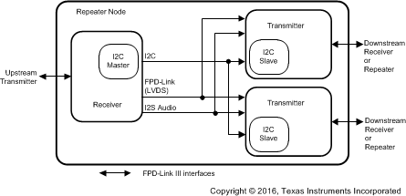
 In a repeater application, the I2C interface at each TX and RX is configured to transparently pass I2C communications upstream or downstream to any I2C device within the system. This includes a mechanism for assigning alternate IDs (Slave Aliases) to downstream devices in the case of duplicate addresses.
 Figure 25. 1:2 Repeater Configuration