ZHCSIG1D August   2016  – September 2023 DS90UB960-Q1

PRODUCTION DATA  

  1.   1
  2. 特性
  3. 应用
  4. 说明
  5. Revision History
  6. Pin Configuration and Functions
    1.     Pin Functions
  7. Specifications
    1. 6.1  Absolute Maximum Ratings
    2. 6.2  ESD Ratings
    3. 6.3  Recommended Operating Conditions
    4. 6.4  Thermal Information
    5. 6.5  DC Electrical Characteristics
    6. 6.6  AC Electrical Characteristics
    7. 6.7  CSI-2 Timing Specifications
    8. 6.8  Recommended Timing for the Serial Control Bus
    9. 6.9  Timing Diagrams
    10. 6.10 Typical Characteristics
  8. Detailed Description
    1. 7.1 Overview
      1. 7.1.1 Functional Description
    2. 7.2 Functional Block Diagram
    3. 7.3 Feature Description
    4. 7.4 Device Functional Modes
      1. 7.4.1  CSI-2 Mode
      2. 7.4.2  RAW Mode
      3. 7.4.3  MODE Pin
      4. 7.4.4  REFCLK
      5. 7.4.5  Receiver Port Control
        1. 7.4.5.1 Video Stream Forwarding
      6. 7.4.6  Input Jitter Tolerance
      7. 7.4.7  Adaptive Equalizer
        1. 7.4.7.1 Transmission Distance
        2. 7.4.7.2 Channel Requirements
        3. 7.4.7.3 Adaptive Equalizer Algorithm
        4. 7.4.7.4 AEQ Settings
          1. 7.4.7.4.1 AEQ Start-Up and Initialization
          2. 7.4.7.4.2 AEQ Range
          3. 7.4.7.4.3 AEQ Timing
          4. 7.4.7.4.4 AEQ Threshold
      8. 7.4.8  Channel Monitor Loop-Through Output Driver
        1. 7.4.8.1 Code Example for CMLOUT FPD3 RX Port 0:
      9. 7.4.9  RX Port Status
        1. 7.4.9.1 RX Parity Status
        2. 7.4.9.2 FPD-Link Decoder Status
        3. 7.4.9.3 RX Port Input Signal Detection
        4. 7.4.9.4 Line Counter
        5. 7.4.9.5 Line Length
      10. 7.4.10 Sensor Status
      11. 7.4.11 GPIO Support
        1. 7.4.11.1 GPIO Input Control and Status
        2. 7.4.11.2 GPIO Output Pin Control
        3. 7.4.11.3 Forward Channel GPIO
        4. 7.4.11.4 Back Channel GPIO
        5. 7.4.11.5 GPIO Pin Status
        6. 7.4.11.6 Other GPIO Pin Controls
      12. 7.4.12 RAW Mode LV / FV Controls
      13. 7.4.13 CSI-2 Protocol Layer
      14. 7.4.14 CSI-2 Short Packet
      15. 7.4.15 CSI-2 Long Packet
      16. 7.4.16 CSI-2 Data Identifier
      17. 7.4.17 Virtual Channel and Context
      18. 7.4.18 CSI-2 Mode Virtual Channel Mapping
        1. 7.4.18.1 Example 1
        2. 7.4.18.2 Example 2:
      19. 7.4.19 CSI-2 Transmitter Frequency
      20. 7.4.20 CSI-2 Output Bandwidth
        1. 7.4.20.1 CSI-2 Output Bandwidth Calculation Example
      21. 7.4.21 CSI-2 Transmitter Status
      22. 7.4.22 Video Buffers
      23. 7.4.23 CSI-2 Line Count and Line Length
      24. 7.4.24 FrameSync Operation
        1. 7.4.24.1 External FrameSync Control
        2. 7.4.24.2 Internally Generated FrameSync
          1. 7.4.24.2.1 Code Example for Internally Generated FrameSync
      25. 7.4.25 CSI-2 Forwarding
        1. 7.4.25.1 Best-Effort Round Robin CSI-2 Forwarding
        2. 7.4.25.2 Synchronized CSI-2 Forwarding
        3. 7.4.25.3 Basic Synchronized CSI-2 Forwarding
          1. 7.4.25.3.1 Code Example for Basic Synchronized CSI-2 Forwarding
        4. 7.4.25.4 Line-Interleaved CSI-2 Forwarding
          1. 7.4.25.4.1 Code Example for Line-Interleaved CSI-2 Forwarding
        5. 7.4.25.5 Line-Concatenated CSI-2 Forwarding
          1. 7.4.25.5.1 Code Example for Line-Concatenated CSI-2 Forwarding
        6. 7.4.25.6 CSI-2 Replicate Mode
        7. 7.4.25.7 CSI-2 Transmitter Output Control
        8. 7.4.25.8 Enabling and Disabling CSI-2 Transmitters
    5. 7.5 Programming
      1. 7.5.1  Serial Control Bus
      2. 7.5.2  Second I2C Port
      3. 7.5.3  I2C Target Operation
      4. 7.5.4  Remote Target Operation
      5. 7.5.5  Remote Target Addressing
      6. 7.5.6  Broadcast Write to Remote Devices
        1. 7.5.6.1 Code Example for Broadcast Write
      7. 7.5.7  I2C Controller Proxy
      8. 7.5.8  I2C Controller Proxy Timing
        1. 7.5.8.1 Code Example for Configuring Fast-Mode Plus I2C Operation
      9. 7.5.9  Interrupt Support
        1. 7.5.9.1 Code Example to Enable Interrupts
        2. 7.5.9.2 FPD-Link III Receive Port Interrupts
        3. 7.5.9.3 Interrupts on Forward Channel GPIO
        4. 7.5.9.4 Interrupts on Change in Sensor Status
        5. 7.5.9.5 Code Example to Readback Interrupts
        6. 7.5.9.6 CSI-2 Transmit Port Interrupts
      10. 7.5.10 Error Handling
        1. 7.5.10.1 Receive Frame Threshold
        2. 7.5.10.2 Port PASS Control
      11. 7.5.11 Timestamp – Video Skew Detection
      12. 7.5.12 Pattern Generation
        1. 7.5.12.1 Reference Color Bar Pattern
        2. 7.5.12.2 Fixed Color Patterns
        3. 7.5.12.3 Pattern Generator Programming
          1. 7.5.12.3.1 Determining Color Bar Size
        4. 7.5.12.4 Code Example for Pattern Generator
      13. 7.5.13 FPD-Link BIST Mode
        1. 7.5.13.1 BIST Operation
    6. 7.6 Register Maps
      1. 7.6.1 Main Registers
      2. 7.6.2 Indirect Access Registers
        1. 7.6.2.1 PATGEN_And_CSI-2 Registers
  9. Application and Implementation
    1. 8.1 Application Information
      1. 8.1.1 Power Over Coax
    2. 8.2 Typical Application
      1. 8.2.1 Design Requirements
      2. 8.2.2 Detailed Design Procedure
      3. 8.2.3 Application Curves
    3. 8.3 System Examples
    4. 8.4 Power Supply Recommendations
      1. 8.4.1 VDD Power Supply
      2. 8.4.2 Power-Up Sequencing
        1. 8.4.2.1 PDB Pin
        2. 8.4.2.2 System Initialization
    5. 8.5 Layout
      1. 8.5.1 Layout Guidelines
        1. 8.5.1.1 Ground
        2. 8.5.1.2 Routing FPD-Link III Signal Traces and PoC Filter
        3. 8.5.1.3 CSI-2 Guidelines
      2. 8.5.2 Layout Example
  10. Device and Documentation Support
    1. 9.1 Documentation Support
      1. 9.1.1 Related Documentation
    2. 9.2 Receiving Notification of Documentation Updates
    3. 9.3 支持资源
    4. 9.4 Trademarks
    5. 9.5 静电放电警告
    6. 9.6 术语表
  11. 10Mechanical, Packaging, and Orderable Information

封装选项

机械数据 (封装 | 引脚)
散热焊盘机械数据 (封装 | 引脚)

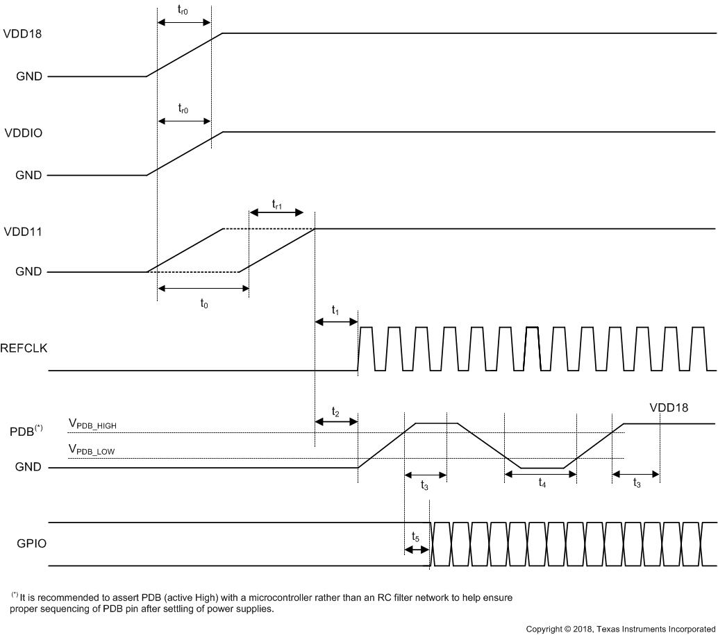
Power-Up Sequencing

The power-up sequence for the DS90UB960-Q1 is as follows:

Table 8-5 Timing Diagram for the Power-Up Sequence
PARAMETERMINTYPMAXUNITNOTES
tr0VDD18 / VDDIO rise time0.2ms@10/90%
tr1VDD11 rise time0.05ms@10/90%
t0VDD18 / VDDIO to VDD11 delay0ms
t1VDDx to REFCLK delay0msKeep REFCLK low until all supplies are up and stable.
t2VDDx to PDB delay0msRelease PDB after all supplies are up and stable.
t3PDB to I2C ready (IDX and MODE valid) delay2ms
t4PDB pulse width2msHard reset
t5PDB to GPIO delay0msKeep GPIOs low or high until PDB is high.
GUID-E18429E5-B681-4AE5-8E85-43B4AF34926B-low.gifFigure 8-18 Power-Up Sequencing