ZHCSIP7B August 2018 – September 2023 DS90UB962-Q1
PRODUCTION DATA
- 1
- 1 特性
- 2 应用
- 3 说明
- 4 Revision History
- 5 Pin Configuration and Functions
-
6 Specifications
- 6.1 Absolute Maximum Ratings
- 6.2 ESD Ratings
- 6.3 Recommended Operating Conditions
- 6.4 Thermal Information
- 6.5 DC Electrical Characteristics
- 6.6 AC Electrical Characteristics
- 6.7 CSI-2 Timing Specifications
- 6.8 Recommended Timing for the Serial Control Bus
- 6.9 Timing Diagrams
- 6.10 Typical Characteristics
-
7 Detailed Description
- 7.1 Overview
- 7.2 Functional Block Diagram
- 7.3 Feature Description
- 7.4
Device Functional Modes
- 7.4.1 CSI-2 Mode
- 7.4.2 RAW Mode
- 7.4.3 MODE Pin
- 7.4.4 REFCLK
- 7.4.5 Receiver Port Control
- 7.4.6 Input Jitter Tolerance
- 7.4.7 Adaptive Equalizer
- 7.4.8 Channel Monitor Loop-Through Output Driver
- 7.4.9 RX Port Status
- 7.4.10 Sensor Status
- 7.4.11 GPIO Support
- 7.4.12 RAW Mode LV / FV Controls
- 7.4.13 CSI-2 Protocol Layer
- 7.4.14 CSI-2 Short Packet
- 7.4.15 CSI-2 Long Packet
- 7.4.16 CSI-2 Data Identifier
- 7.4.17 Virtual Channel and Context
- 7.4.18 CSI-2 Mode Virtual Channel Mapping
- 7.4.19 CSI-2 Transmitter Frequency
- 7.4.20 CSI-2 Output Bandwidth
- 7.4.21 CSI-2 Transmitter Status
- 7.4.22 Video Buffers
- 7.4.23 CSI-2 Line Count and Line Length
- 7.4.24 FrameSync Operation
- 7.4.25
CSI-2 Forwarding
- 7.4.25.1 Best-Effort Round Robin CSI-2 Forwarding
- 7.4.25.2 Synchronized CSI-2 Forwarding
- 7.4.25.3 Basic Synchronized CSI-2 Forwarding
- 7.4.25.4 Line-Interleaved CSI-2 Forwarding
- 7.4.25.5 Line-Concatenated CSI-2 Forwarding
- 7.4.25.6 CSI-2 Transmitter Output Control
- 7.4.25.7 Enabling and Disabling CSI-2 Transmitters
- 7.5
Programming
- 7.5.1 Serial Control Bus
- 7.5.2 Second I2C Port
- 7.5.3 I2C Target Operation
- 7.5.4 Remote Target Operation
- 7.5.5 Remote Target Addressing
- 7.5.6 Broadcast Write to Remote Devices
- 7.5.7 I2C Controller Proxy
- 7.5.8 I2C Controller Proxy Timing
- 7.5.9 Interrupt Support
- 7.5.10 Error Handling
- 7.5.11 Timestamp – Video Skew Detection
- 7.5.12 Pattern Generation
- 7.5.13 FPD-Link BIST Mode
- 7.6 Register Maps
- 8 Application and Implementation
- 9 Device and Documentation Support
- 10Mechanical, Packaging, and Orderable Information
7.5.1 Serial Control Bus
The DS90UB962-Q1 implements two I2C-compatible serial control buses. Both I2C ports support local device configuration and incorporate a bidirectional control channel (BCC) that allows communication with a remote serializers as well as remote I2C target devices.
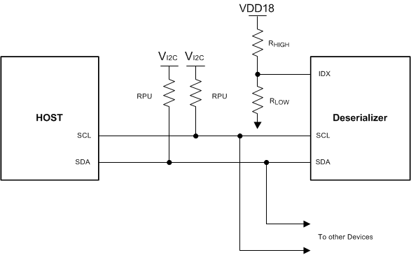
The device address is set through a resistor divider connected to the IDx pin (R1 and R2 – see Figure 7-18).
 Figure 7-18 Serial Control Bus Connection
The serial control bus consists of two signals, SCL and SDA. SCL is a Serial Bus Clock Input. SDA is the Serial Bus Data Input / Output signal. Both SCL and SDA signals require an external pullup resistor to VI2C, where VI2C is a voltage rail that matches the voltage applied to VDDIO. The pull-up resistor value may be adjusted to account for capacitive loading and data rate requirements. Refer to "I2C Bus Pullup Resistor Calculation" (SLVA689) to determine the pull-up resistor value to VI2C. The signals are either pulled High, or driven Low.
The IDX pin configures the control interface to one of eight possible device addresses. A pullup resistor and a pulldown resistor may be used to set the appropriate voltage ratio between the IDX input pin (VIDX) and V(VDD18), each ratio corresponding to a specific device address. See Table 7-18, Serial Control Bus Addresses for IDX.
| NO. | VIDX VOLTAGE RANGE | VIDX TARGET VOLTAGE | SUGGESTED STRAP RESISTORS (1% TOL) | PRIMARY ASSIGNED I2C ADDRESS | ||||
|---|---|---|---|---|---|---|---|---|
| VMIN | VTYP | VMAX | VDD18 = 1.80 V | RHIGH ( kΩ ) | RLOW ( kΩ ) | 7-BIT | 8-BIT | |
| 0 | 0 | 0 | 0.131 × V(VDD18) | 0 | OPEN | 10.0 | 0x30 | 0x60 |
| 1 | 0.179 × V(VDD18) | 0.213 × V(VDD18) | 0.247 × V(VDD18) | 0.374 | 88.7 | 23.2 | 0x32 | 0x64 |
| 2 | 0.296 × V(VDD18) | 0.330 × V(VDD18) | 0.362 × V(VDD18) | 0.582 | 75.0 | 35.7 | 0x34 | 0x68 |
| 3 | 0.412 × V(VDD18) | 0.443 × V(VDD18) | 0.474 × V(VDD18) | 0.792 | 71.5 | 56.2 | 0x36 | 0x6C |
| 4 | 0.525 × V(VDD18) | 0.559 × V(VDD18) | 0.592 × V(VDD18) | 0.995 | 78.7 | 97.6 | 0x38 | 0x70 |
| 5 | 0.642 × V(VDD18) | 0.673 × V(VDD18) | 0.704 × V(VDD18) | 1.202 | 39.2 | 78.7 | 0x3A | 0x74 |
| 6 | 0.761 × V(VDD18) | 0.792 × V(VDD18) | 0.823 × V(VDD18) | 1.420 | 25.5 | 95.3 | 0x3C | 0x78 |
| 7 | 0.876 × V(VDD18) | V(VDD18) | V(VDD18) | 1.8 | 10.0 | OPEN | 0x3D | 0x7A |
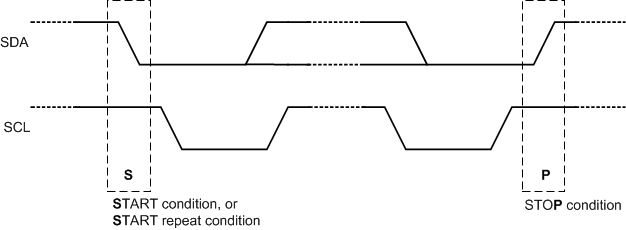
The Serial Bus protocol is controlled by START, START-Repeated, and STOP phases. A START occurs when SDA transitions Low while SCL is High. A STOP occurs when SDA transitions High while SCL is also HIGH. See Figure 7-19.
 Figure 7-19 START and STOP Conditions
To communicate with a remote device, the host controller sends the target address and listens for a response from the target. This response is referred to as an acknowledge bit (ACK). If a target on the bus is addressed correctly, it acknowledges (ACKs) the controller by driving the SDA bus low. If the address does not match one of the target addresses of the device, it not-acknowledges (NACKs) the controller by letting SDA be pulled High. ACKs can also occur on the bus when data transmissions are in process. When the controller is writing data, the target ACKs after every data byte is successfully received. When the controller is reading data, the controller ACKs after every data byte is received to let the target know it wants to receive another data byte. When the controller wants to stop reading, it NACKs after the last data byte and creates a stop condition on the bus. All communication on the bus begins with either a Start condition or a Repeated Start condition. All communication on the bus ends with a Stop condition. A READ is shown in Figure 7-20 and a WRITE is shown in Figure 7-21.
 Figure 7-20 Serial Control Bus — READ
 Figure 7-21 Serial Control Bus — WRITE
 Figure 7-22 Basic
Operation
Figure 7-22 Basic
OperationThe I2C Controller located at the Deserializer must support I2C clock stretching. For more information on I2C interface requirements and throughput considerations, refer to I2C Communication Over FPD-Link III With Bidirectional Control Channel (SNLA131) and I2C over DS90UB913/4 FPD-Link III With Bidirectional Control Channel (SNLA222).