ZHCSIP7B August 2018 – September 2023 DS90UB962-Q1
PRODUCTION DATA
- 1
- 1 特性
- 2 应用
- 3 说明
- 4 Revision History
- 5 Pin Configuration and Functions
-
6 Specifications
- 6.1 Absolute Maximum Ratings
- 6.2 ESD Ratings
- 6.3 Recommended Operating Conditions
- 6.4 Thermal Information
- 6.5 DC Electrical Characteristics
- 6.6 AC Electrical Characteristics
- 6.7 CSI-2 Timing Specifications
- 6.8 Recommended Timing for the Serial Control Bus
- 6.9 Timing Diagrams
- 6.10 Typical Characteristics
-
7 Detailed Description
- 7.1 Overview
- 7.2 Functional Block Diagram
- 7.3 Feature Description
- 7.4
Device Functional Modes
- 7.4.1 CSI-2 Mode
- 7.4.2 RAW Mode
- 7.4.3 MODE Pin
- 7.4.4 REFCLK
- 7.4.5 Receiver Port Control
- 7.4.6 Input Jitter Tolerance
- 7.4.7 Adaptive Equalizer
- 7.4.8 Channel Monitor Loop-Through Output Driver
- 7.4.9 RX Port Status
- 7.4.10 Sensor Status
- 7.4.11 GPIO Support
- 7.4.12 RAW Mode LV / FV Controls
- 7.4.13 CSI-2 Protocol Layer
- 7.4.14 CSI-2 Short Packet
- 7.4.15 CSI-2 Long Packet
- 7.4.16 CSI-2 Data Identifier
- 7.4.17 Virtual Channel and Context
- 7.4.18 CSI-2 Mode Virtual Channel Mapping
- 7.4.19 CSI-2 Transmitter Frequency
- 7.4.20 CSI-2 Output Bandwidth
- 7.4.21 CSI-2 Transmitter Status
- 7.4.22 Video Buffers
- 7.4.23 CSI-2 Line Count and Line Length
- 7.4.24 FrameSync Operation
- 7.4.25
CSI-2 Forwarding
- 7.4.25.1 Best-Effort Round Robin CSI-2 Forwarding
- 7.4.25.2 Synchronized CSI-2 Forwarding
- 7.4.25.3 Basic Synchronized CSI-2 Forwarding
- 7.4.25.4 Line-Interleaved CSI-2 Forwarding
- 7.4.25.5 Line-Concatenated CSI-2 Forwarding
- 7.4.25.6 CSI-2 Transmitter Output Control
- 7.4.25.7 Enabling and Disabling CSI-2 Transmitters
- 7.5
Programming
- 7.5.1 Serial Control Bus
- 7.5.2 Second I2C Port
- 7.5.3 I2C Target Operation
- 7.5.4 Remote Target Operation
- 7.5.5 Remote Target Addressing
- 7.5.6 Broadcast Write to Remote Devices
- 7.5.7 I2C Controller Proxy
- 7.5.8 I2C Controller Proxy Timing
- 7.5.9 Interrupt Support
- 7.5.10 Error Handling
- 7.5.11 Timestamp – Video Skew Detection
- 7.5.12 Pattern Generation
- 7.5.13 FPD-Link BIST Mode
- 7.6 Register Maps
- 8 Application and Implementation
- 9 Device and Documentation Support
- 10Mechanical, Packaging, and Orderable Information
7.4.24.2 Internally Generated FrameSync
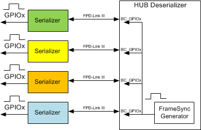
In Internal FrameSync mode, an internally generated FrameSync signal is sent to one or more of the attached FPD3 Serializers through a GPIO signal in the back channel.
FrameSync operation is controlled by the FS_CTL, FS_HIGH_TIME_x, and FS_LOW_TIME_x 0x18 – 0x1C registers. The resolution of the FrameSync generator clock (FS_CLK_PD) is derived from the back channel frame period (BC_FREQ_SELECT register). For each 2.5-Mbps back channel operation, the frame period is 12 µs (30 bits × 400 ns/bit).
Once enabled, the FrameSync signal is sent continuously based on the programmed conditions.
Enabling the internal FrameSync mode is done by setting the FS_GEN_ENABLE control in the FS_CTL register to a value of 1. The FS_MODE field controls the clock source used for the FrameSync generation. The FS_GEN_MODE field configures whether the duty cycle of the FrameSync is 50/50 or whether the high and low periods are controlled separately. The FrameSync high and low periods are controlled by the FS_HIGH_TIME and FS_LOW_TIME registers.
The accuracy of the internally generated FrameSync is directly dependent on the accuracy of the 25-MHz oscillator used as the reference clock.
 Figure 7-13 Internal FrameSync
 Figure 7-14 Internal FrameSync Signal
The following example shows generation of a FrameSync signal at 60 pulses per second. Mode settings:
- Programmable High/Low periods: FS_GEN_MODE 0x18[1]=0
- Use port 0 back channel frame period: FS_MODE 0x18[7:4]=0x0
- Back channel rate of 50 Mbps: BC_FREQ_SELECT for port 0 0x58[2:0]=110b
- Initial FS state of 0: FS_INIT_STATE 0x18[2]=0
Based on mode settings, the FrameSync is generated based upon FS_CLK_PD of 12 us.
The total period of the FrameSync is (1 sec / 60 hz) / 600 ns or approximately 27,778 counts.
For a 10% duty cycle, set the high time to 2,776 (0x0AD7) cycles, and the low time to 24,992 (0x61A0) cycles:
- FS_HIGH_TIME_1: 0x19=0x0A
- FS_HIGH_TIME_0: 0x1A=0xD7
- FS_LOW_TIME_1: 0x1B=0x61
- FS_LOW_TIME_0: 0x1C=0xA0