ZHCSEN8A NOVEMBER 2014 – January 2016 DS90UH940-Q1
PRODUCTION DATA.
- 1 特性
- 2 应用
- 3 说明
- 4 应用 图
- 5 修订历史记录
- 6 Pin Configurations and Functions
-
7 Specifications
- 7.1 Absolute Maximum Ratings
- 7.2 ESD Ratings—JEDEC
- 7.3 ESD Ratings—IEC and ISO
- 7.4 Recommended Operating Conditions
- 7.5 Thermal Information
- 7.6 DC Electrical Characteristics
- 7.7 AC Electrical Characteristics
- 7.8 Timing Requirements for the Serial Control Bus
- 7.9 Switching Characteristics
- 7.10 Timing Diagrams and Test Circuits
- 7.11 Power Sequence
- 7.12 Typical Characteristics
-
8 Detailed Description
- 8.1 Overview
- 8.2 Functional Block Diagram
- 8.3
Feature Description
- 8.3.1 High Speed Forward Channel Data Transfer
- 8.3.2 Low Speed Back Channel Data Transfer
- 8.3.3 FPD-Link III Port Register Access
- 8.3.4 Clock and Output Status
- 8.3.5 LVCMOS VDDIO Option
- 8.3.6 Power Down (PDB)
- 8.3.7 Interrupt Pin — Functional Description and Usage (INTB_IN)
- 8.3.8 General-purpose I/O
- 8.3.9 SPI Communication
- 8.3.10 Backward Compatibility
- 8.3.11 Input Equalization
- 8.3.12 I2S Audio Interface
- 8.3.13 HDCP
- 8.3.14 Built-In Self Test (BIST)
- 8.3.15 Internal Pattern Generation
- 8.4 Device Functional Modes
- 8.5
Programming
- 8.5.1 Serial Control Bus
- 8.5.2 Multi-Master Arbitration Support
- 8.5.3 I2C Restrictions on Multi-Master Operation
- 8.5.4 Multi-Master Access to Device Registers for Newer FPD-Link III Devices
- 8.5.5 Multi-Master Access to Device Registers for Older FPD-Link III Devices
- 8.5.6 Restrictions on Control Channel Direction for Multi-Master Operation
- 8.6 Register Maps
- 9 Application and Implementation
- 10Power Supply Recommendations
- 11Layout
- 12器件和文档支持
- 13机械、封装和可订购信息
9 Application and Implementation
NOTE
Information in the following applications sections is not part of the TI component specification, and TI does not warrant its accuracy or completeness. TI’s customers are responsible for determining suitability of components for their purposes. Customers should validate and test their design implementation to confirm system functionality.
9.1 Application Information
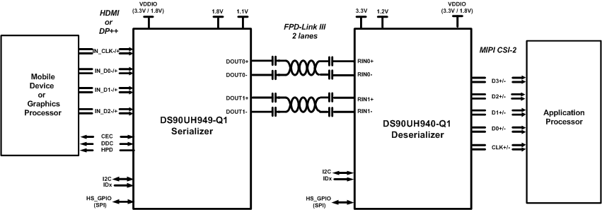
The DS90UH940-Q1 is a FPD-Link III Deserializer which, in conjunction with the DS90UH949/947-Q1 Serializers, converts 1-lane or 2-lane FPD-Link III streams into a MIPI CSI-2 interface. The Deserializer is capable of operating over cost-effective 50Ω single-ended coaxial or 100Ω differential shielded twisted-pair (STP) cables. It recovers the data from two FPD-Link III serial streams and translates it into a Camera Serial Interface (CSI-2) format compatible with MIPI DPHY/CSI-2 supporting video resolutions up to WUXGA and 1080p60 with 24-bit color depth.
9.2 Typical Applications
Bypass capacitors should be placed near the power supply pins. At a minimum, four (4) 10µF capacitors should be used for local device bypassing. Ferrite beads are placed on the two sets of supply pins (VDD33 and VDDIO ) for effective noise suppression. The interface to the graphics source is LVDS. The VDDIO pins may be connected to 3.3V or 1.8V. A capacitor and resistor are placed on the PDB pin to delay the enabling of the device until power is stable. See Figure 37 for a typical STP connection diagram and for a typical coax connection diagram.
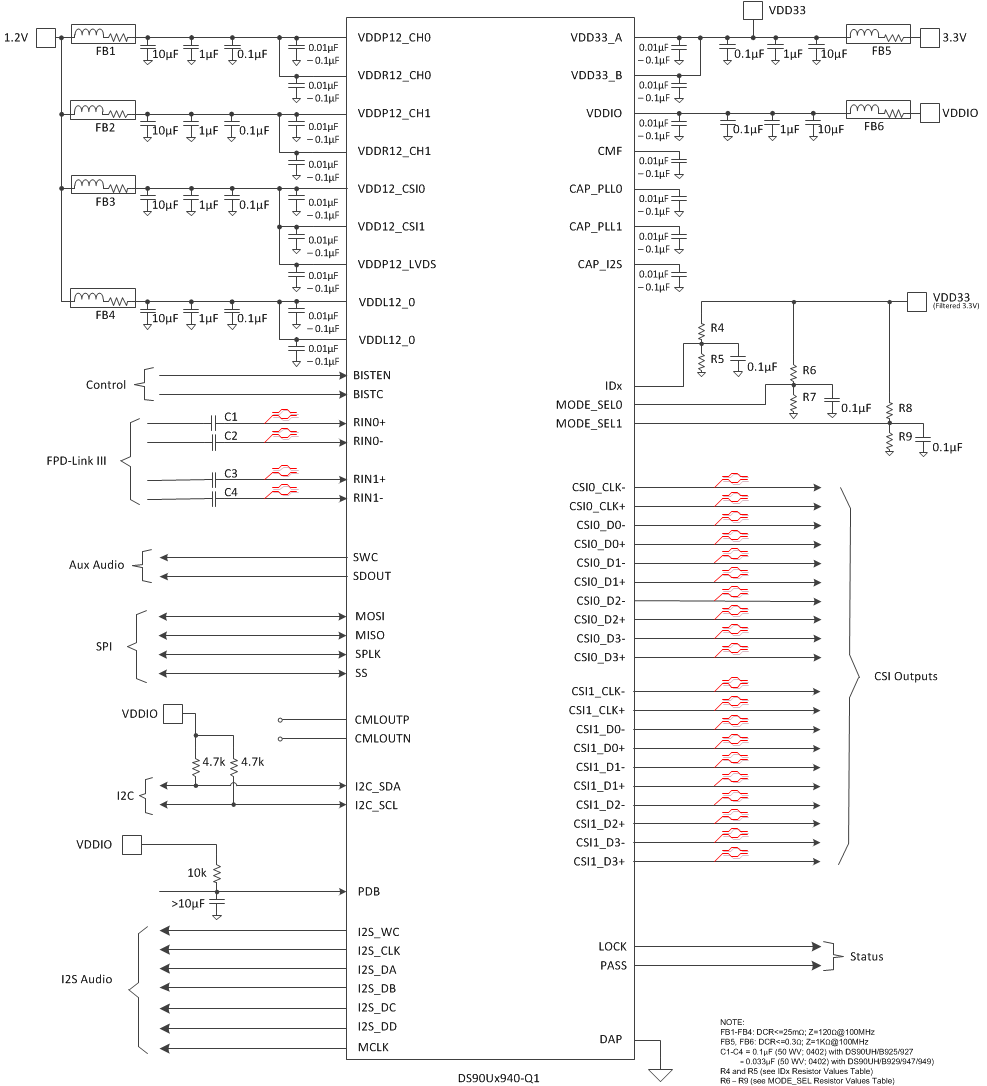 Figure 37. Typical Connection Diagram (STP)
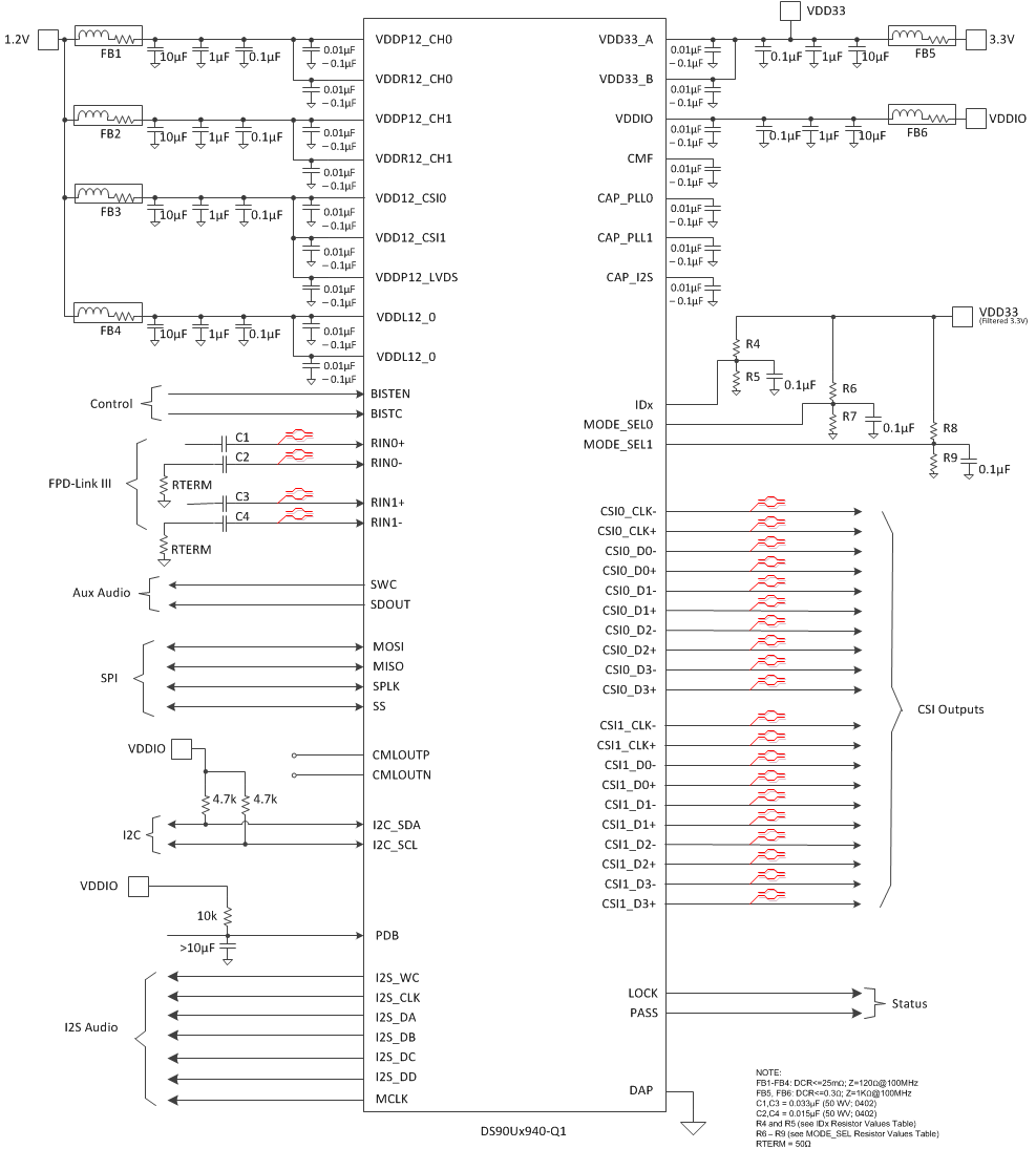 Figure 38. Typical Connection Diagram (Coax)
9.2.1 Design Requirements
For the typical design application, use the following as input parameters.
Table 14. Design Parameters
| Design Parameter | Example Value |
|---|---|
| VDDIO | 1.8V or 3.3V |
| VDD12 | 1.2V |
| VDD33 | 3.3V |
| AC Coupling Capacitor for RIN0± and RIN1± | 33 nF |
The SER/DES supports only AC-coupled interconnects through an integrated DC-balanced decoding scheme. External AC coupling capacitors must be placed in series in the FPD-Link III signal path as illustrated in Figure 39. For applications utilizing single-ended 50 Ω coaxial cable, the unused data pins (RIN0-, RIN1-) should utilize a 15 nF capacitor and should be terminated with a 50 Ω resistor.
 Figure 39. AC-Coupled Connection (STP)
 Figure 40. AC-Coupled Connection (Coaxial)
For high-speed FPD–Link III transmissions, the smallest available package should be used for the AC coupling capacitor. This will help minimize degradation of signal quality due to package parasitics. The I/O’s require 33 nF AC coupling capacitors to the line.
9.2.2 Detailed Design Procedure
9.2.2.1 PCB Layout and Power System Considerations
Circuit board layout and stack-up for the LVDS serializer and deserializer devices should be designed to provide low-noise power to the device. Good layout practice will also separate high frequency or high-level inputs and outputs to minimize unwanted stray noise, feedback and interference. Power system performance may be greatly improved by using thin dielectrics (2 to 4 mil) for power / ground sandwiches. This arrangement utilizes the plane capacitance for the PCB power system and has low-inductance, which has proven effectiveness especially at high frequencies, and makes the value and placement of external bypass capacitors less critical. External bypass capacitors should include both RF ceramic and tantalum electrolytic types. RF capacitors may use values in the range of 0.01 μF to 10 μF. Tantalum capacitors may be in the 2.2 μF to 10 μF range. The voltage rating of the tantalum capacitors should be at least 5X the power supply voltage being used.
MLCC surface mount capacitors are recommended due to their smaller parasitic properties. When using multiple capacitors per supply pin, locate the smaller value closer to the pin. A large bulk capacitor is recommended at the point of power entry. This is typically in the 50 μF to 100 μF range and will smooth low frequency switching noise. It is recommended to connect power and ground pins directly to the power and ground planes with bypass capacitors connected to the plane with via on both ends of the capacitor. Connecting power or ground pins to an external bypass capacitor will increase the inductance of the path. A small body size X7R chip capacitor, such as 0603 or 0805, is recommended for external bypass. A small body sized capacitor has less inductance. The user must pay attention to the resonance frequency of these external bypass capacitors, usually in the range of 20MHz-30MHz. To provide effective bypassing, multiple capacitors are often used to achieve low impedance between the supply rails over the frequency of interest. At high frequency, it is also a common practice to use two vias from power and ground pins to the planes, reducing the impedance at high frequency.
Use at least a four layer board with a power and ground plane. Locate LVCMOS signals away from the LVDS lines to prevent coupling from the LVCMOS lines to the LVDS lines. Closely coupled differential lines of 100 Ω are typically recommended for LVDS interconnect. The closely coupled lines help to ensure that coupled noise will appear as common mode and thus is rejected by the receivers. The tightly coupled lines will also radiate less.
At least 32 thermal vias are necessary from the device center DAP to the ground plane. They connect the device ground to the PCB ground plane, as well as conduct heat from the exposed pad of the package to the PCB ground plane. More information on the WQFN style package, including PCB design and manufacturing requirements, is provided in TI Application Note: AN-1187.
9.2.2.2 CML Interconnect Guidelines
See AN-1108 and AN-905 for full details.
- Use 100Ω coupled differential pairs
- Use the S/2S/3S rule in spacings
- S = space between the pair
- 2S = space between pairs
- 3S = space to LVCMOS signal
- Minimize the number of Vias
- Use differential connectors when operating above 500Mbps line speed
- Maintain balance of the traces
- Minimize skew within the pair
- Terminate as close to the TX outputs and RX inputs as possible
Additional general guidance can be found in the LVDS Owner’s Manual - available in PDF format from the Texas Instruments web site at: SNLA187
9.2.3 Application Performance Plots
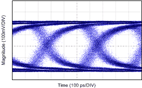
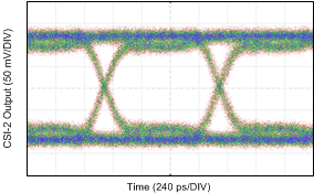
The plots below correspond to 1080p60 video application with 2-lane FPD-Link III input and MIPI 4 lanes output.
