ZHCSD35B November 2014 – August 2019 DS90UH949-Q1
PRODUCTION DATA.
- 1 特性
- 2 应用
- 3 说明
- 4 修订历史记录
- 5 Pin Configuration and Functions
-
6 Specifications
- 6.1 Absolute Maximum Ratings
- 6.2 ESD Ratings
- 6.3 Recommended Operating Conditions
- 6.4 Thermal Information
- 6.5 DC Electrical Characteristics
- 6.6 AC Electrical Characteristics
- 6.7 DC And AC Serial Control Bus Characteristics
- 6.8 Recommended Timing for the Serial Control Bus
- 6.9 Timing Diagrams
- 6.10 Typical Characteristics
-
7 Detailed Description
- 7.1 Overview
- 7.2 Functional Block Diagram
- 7.3
Feature Description
- 7.3.1 High-Definition Multimedia Interface (HDMI)
- 7.3.2 Transition Minimized Differential Signaling
- 7.3.3 Enhanced Display Data Channel
- 7.3.4 Extended Display Identification Data (EDID)
- 7.3.5 Consumer Electronics Control (CEC)
- 7.3.6 +5-V Power Signal
- 7.3.7 Hot Plug Detect (HPD)
- 7.3.8 High-Speed Forward Channel Data Transfer
- 7.3.9 Back Channel Data Transfer
- 7.3.10 FPD-Link III Port Register Access
- 7.3.11 Power Down (PDB)
- 7.3.12 Serial Link Fault Detect
- 7.3.13 Interrupt Pin (INTB)
- 7.3.14 Remote Interrupt Pin (REM_INTB)
- 7.3.15 General-Purpose I/O
- 7.3.16 SPI Communication
- 7.3.17 Backward Compatibility
- 7.3.18 Audio Modes
- 7.3.19 HDCP
- 7.3.20 Built-In Self Test (BIST)
- 7.3.21 Internal Pattern Generation
- 7.3.22 Spread Spectrum Clock Tolerance
- 7.4 Device Functional Modes
- 7.5
Programming
- 7.5.1 Serial Control Bus
- 7.5.2 Multi-Master Arbitration Support
- 7.5.3 I2C Restrictions on Multi-Master Operation
- 7.5.4 Multi-Master Access to Device Registers for Newer FPD-Link III Devices
- 7.5.5 Multi-Master Access to Device Registers for Older FPD-Link III Devices
- 7.5.6 Restrictions on Control Channel Direction for Multi-Master Operation
- 7.6 Register Maps
- 8 Application and Implementation
- 9 Power Supply Recommendations
- 10Layout
- 11器件和文档支持
- 12机械、封装和可订购信息
7.3.16.3 Reverse Channel SPI Operation
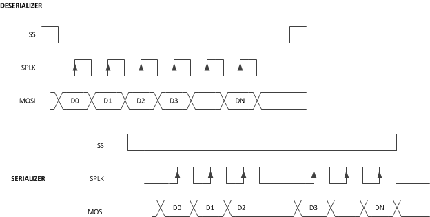
In Reverse Channel SPI operation, the Deserializer samples the Slave Select (SS), SPI clock (SCLK) into the internal oscillator clock domain. In addition, upon detection of the active SPI clock edge, the Deserializer samples the SPI data (MOSI). The SPI data samples are stored in a buffer to be passed to the Serializer over the back channel. The Deserializer sends SPI information in a back channel frame to the Serializer. In each back channel frame, the Deserializer sends an indication of the Slave Select value. The Slave Select should be inactive (high) for at least one back-channel frame period to ensure propagation to the Serializer.
Because data is delivered in separate back channel frames and buffered, the data may be regenerated in bursts. Figure 13 shows an example of the SPI data regeneration when the data arrives in three back channel frames. The first frame delivered the SS active indication, the second frame delivered the first three data bits, and the third frame delivers the additional data bits.
 Figure 13. Reverse Channel SPI Write
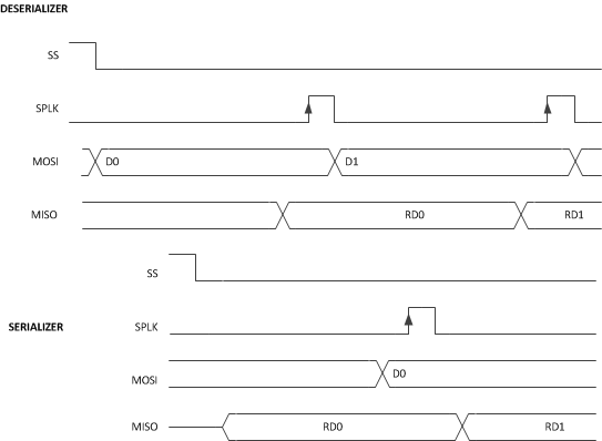
 For Reverse Channel SPI reads, the SPI master must wait for a round-trip response before generating the sampling edge of the SPI clock. This is similar to operation in Forward channel mode. Note that at most one data/clock sample will be sent per back channel frame.
 Figure 14. Reverse Channel SPI Read
 For both Reverse Channel SPI writes and reads, the SPI_SS signal should be deasserted for at least one back channel frame period.
Table 4. SPI SS Deassertion Requirement
| BACK CHANNEL FREQUENCY | DEASSERTION REQUIREMENT |
|---|---|
| 5 Mbps | 7.5 µs |
| 10 Mbps | 3.75 µs |
| 20 Mbps | 1.875 µs |