SNLS325D May 2010 – December 2016 DS92LV0421 , DS92LV0422
PRODUCTION DATA.
- 1 Features
- 2 Applications
- 3 Description
- 4 Revision History
- 5 Pin Configuration and Functions
-
6 Specifications
- 6.1 Absolute Maximum Ratings
- 6.2 ESD Ratings
- 6.3 Recommended Operating Conditions
- 6.4 Thermal Information
- 6.5 Electrical Characteristics: Serializer DC
- 6.6 Electrical Characteristics: Deserializer DC
- 6.7 Electrical Characteristics: DC and AC Serial Control Bus
- 6.8 Timing Requirements: Serial Control Bus
- 6.9 Switching Characteristics: Serializer
- 6.10 Switching Characteristics: Deserializer
- 6.11 Typical Characteristics
-
7 Detailed Description
- 7.1 Overview
- 7.2 Functional Block Diagrams
- 7.3
Feature Description
- 7.3.1 Parallel LVDS Data Transfer (Color Bit Mapping Select)
- 7.3.2 Serial Data Transfer
- 7.3.3 Video Control Signal Filter
- 7.3.4 Serializer Functional Description
- 7.3.5
Deserializer Functional Description
- 7.3.5.1 Signal Quality Enhancers
- 7.3.5.2 EMI Reduction Features
- 7.3.5.3 Deserializer Clock-Data Recovery Status Flag (LOCK), Output Enable (OEN), and Output State Select (OSS_SEL)
- 7.3.5.4 Deserializer Oscillator Output (Optional)
- 7.3.6 Built-In Self Test (BIST)
- 7.3.7 Optional Serial Bus Control
- 7.4 Device Functional Modes
- 7.5 Register Maps
- 8 Application and Implementation
- 9 Power Supply Recommendations
- 10Layout
- 11Device and Documentation Support
- 12Mechanical, Packaging, and Orderable Information
封装选项
请参考 PDF 数据表获取器件具体的封装图。
机械数据 (封装 | 引脚)
- RHS|48
散热焊盘机械数据 (封装 | 引脚)
- RHS|48
订购信息
1 Features
- 5-Channel (4 Data + 1 Clock) Channel Link LVDS Parallel Interface Supports 24-Bit Data 3-Bit Control at 10 to 75 MHz
- AC-Coupled STP Interconnect Up to 10 m
- Integrated Terminations on Serializer and Deserializer
- At-Speed Link BIST Mode and Reporting Pin
- Optional I2C-Compatible Serial Control Bus
- Power-Down Mode Minimizes Power Dissipation
- 1.8-V or 3.3-V Compatible LVCMOS I/O Interface
- >8-kV HBM
- –40° to 85°C Temperature Range
- Serializer (DS92LV0421)
- Data Scrambler for Reduced EMI
- DC–Balance Encoder for AC Coupling
- Selectable Output VOD and Adjustable De-Emphasis
- Deserializer (DS92LV0422)
- Fast Random Data Lock; No Reference Clock Required
- Adjustable Input Receiver Equalization
- EMI Minimization on Output Parallel Bus (SSCG and LVDS VOD Select)
2 Applications
- Embedded Video and Displays
- Medical Imaging and Factory Automation
- Office Automation (Printers and Scanners)
- Security and Video Surveillance
- General-Purpose Data Communication
3 Description
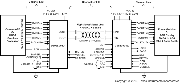
The DS92LV042x chipset translates a Channel Link LVDS video interface (4 LVDS Data + LVDS Clock) into a high-speed serialized interface over a single CML pair. The DS92LV042x enables applications currently using popular Channel Link or OpenLDI LVDS style devices to upgrade seamlessly to an embedded clock interface. This serial bus scheme reduces interconnect cost and eases design challenges. The parallel OpenLDI LVDS interface also reduces FPGA I/O pins, board trace count, and alleviates EMI issues when compared to traditional single-ended wide bus interfaces.
Programmable transmit de-emphasis, receive equalization, on-chip scrambling, and DC-balancing enables longer distance transmission over lossy cables and backplanes. The DS92LV0422 automatically locks to incoming data without an external reference clock or special sync patterns, providing easy plug-and-go operation.
The DS92LV042x chipset is programmable through an I2C interface as well as through pins. A built-in, at-speed BIST feature validates link integrity and may be used for system diagnostics. The DS92LV0421 and DS92LV0422 can be used interchangeably with the DS92LV2421 or DS92LV2422. This allows designers the flexibility to connect to the host device and receiving devices with different interface types: LVDS or LVCMOS.
Device Information(1)
| PART NUMBER | PACKAGE | BODY SIZE (NOM) |
|---|---|---|
| DS92LV0421 | WQFN (36) | 6.00 mm × 6.00 mm |
| DS92LV0422 | WQFN (48) | 7.00 mm × 7.00 mm |
- For all available packages, see the orderable addendum at the end of the data sheet.
Typical Application Block Diagram
