SNLS325D May 2010 – December 2016 DS92LV0421 , DS92LV0422
PRODUCTION DATA.
- 1 Features
- 2 Applications
- 3 Description
- 4 Revision History
- 5 Pin Configuration and Functions
-
6 Specifications
- 6.1 Absolute Maximum Ratings
- 6.2 ESD Ratings
- 6.3 Recommended Operating Conditions
- 6.4 Thermal Information
- 6.5 Electrical Characteristics: Serializer DC
- 6.6 Electrical Characteristics: Deserializer DC
- 6.7 Electrical Characteristics: DC and AC Serial Control Bus
- 6.8 Timing Requirements: Serial Control Bus
- 6.9 Switching Characteristics: Serializer
- 6.10 Switching Characteristics: Deserializer
- 6.11 Typical Characteristics
-
7 Detailed Description
- 7.1 Overview
- 7.2 Functional Block Diagrams
- 7.3
Feature Description
- 7.3.1 Parallel LVDS Data Transfer (Color Bit Mapping Select)
- 7.3.2 Serial Data Transfer
- 7.3.3 Video Control Signal Filter
- 7.3.4 Serializer Functional Description
- 7.3.5
Deserializer Functional Description
- 7.3.5.1 Signal Quality Enhancers
- 7.3.5.2 EMI Reduction Features
- 7.3.5.3 Deserializer Clock-Data Recovery Status Flag (LOCK), Output Enable (OEN), and Output State Select (OSS_SEL)
- 7.3.5.4 Deserializer Oscillator Output (Optional)
- 7.3.6 Built-In Self Test (BIST)
- 7.3.7 Optional Serial Bus Control
- 7.4 Device Functional Modes
- 7.5 Register Maps
- 8 Application and Implementation
- 9 Power Supply Recommendations
- 10Layout
- 11Device and Documentation Support
- 12Mechanical, Packaging, and Orderable Information
封装选项
请参考 PDF 数据表获取器件具体的封装图。
机械数据 (封装 | 引脚)
- RHS|48
散热焊盘机械数据 (封装 | 引脚)
- RHS|48
订购信息
8 Application and Implementation
NOTE
Information in the following applications sections is not part of the TI component specification, and TI does not warrant its accuracy or completeness. TI’s customers are responsible for determining suitability of components for their purposes. Customers should validate and test their design implementation to confirm system functionality.
8.1 Application Information
8.1.1 Display Application
The DS92LV042x chipset is intended for interface between a host (graphics processor) and a display. It supports a 24-bit color depth (RGB888) and up to 1024 × 768 display formats. In a RGB888 application, 24 color bits (R[7:0], G[7:0], and B[7:0]), Pixel Clock (PCLK), and three control bits (VS, HS, and DE) are supported across the serial link with RXCLKIN rates from 10 to 75 MHz. The chipset may also be used in 18-bit color applications. In this application, three to six general-purpose signals may also be sent from host to display.
8.1.2 Live Link Insertion
The serializer and deserializer devices support live link or cable hot plug applications. The automatic receiver lock to random data plug and go hot insertion capability allows the DS92LV0422 to attain lock to the active data stream during a live insertion event.
8.1.3 Alternate Color or Data Mapping
Color-mapped data pin names are provided to specify a recommended mapping for 24-bit and 18-bit applications. Seven (7) is assumed to be the MSB, and Zero (0) is assumed to be the LSB. While this is recommended, it is not required. When connecting to earlier generations of FPD-Link II serializer and deserializer devices, a color mapping review is recommended to ensure the correct connectivity is obtained. Table 14 provides examples for interfacing between DS92LV0421 and different deserializers. Table 15 provides examples for interfacing between DS92LV0422 and different serializers.
Table 14. Serializer Alternate Color or Data Mapping
| CHANNEL LINK | BIT NUMBER | RGB (LSB EXAMPLE) | DS92LV2422 | DS90UR124 | DS99R124Q-Q1 | DS90C124 |
|---|---|---|---|---|---|---|
| RXIN3 | Bit 26 | B1 | B1 | N/A | N/A | N/A |
| Bit 25 | B0 | B0 | ||||
| Bit 24 | G1 | G1 | ||||
| Bit 23 | G0 | G0 | ||||
| Bit 22 | R1 | R1 | ||||
| Bit 21 | R0 | R0 | ||||
| RXIN2 | Bit 20 | DE | DE | ROUT20 | TXOUT2 | ROUT20 |
| Bit 19 | VS | VS | ROUT19 | ROUT19 | ||
| Bit 18 | HS | HS | ROUT18 | ROUT18 | ||
| Bit 17 | B7 | B7 | ROUT17 | ROUT17 | ||
| Bit 16 | B6 | B6 | ROUT16 | ROUT16 | ||
| Bit 15 | B5 | B5 | ROUT15 | ROUT15 | ||
| Bit 14 | B4 | B4 | ROUT14 | ROUT14 | ||
| RXIN1 | Bit 13 | B3 | B3 | ROUT13 | TXOUT1 | ROUT13 |
| Bit 12 | B2 | B2 | ROUT12 | ROUT12 | ||
| Bit 11 | G7 | G7 | ROUT11 | ROUT11 | ||
| Bit 10 | G6 | G6 | ROUT10 | ROUT10 | ||
| Bit 9 | G5 | G5 | ROUT9 | ROUT9 | ||
| Bit 8 | G4 | G4 | ROUT8 | ROUT8 | ||
| Bit 7 | G3 | G3 | ROUT7 | ROUT7 | ||
| RXIN0 | Bit 6 | G2 | G2 | ROUT6 | TXOUT0 | ROUT6 |
| Bit 5 | R7 | R7 | ROUT5 | ROUT5 | ||
| Bit 4 | R6 | R6 | ROUT4 | ROUT4 | ||
| Bit 3 | R5 | R5 | ROUT3 | ROUT3 | ||
| Bit 2 | R4 | R4 | ROUT2 | ROUT2 | ||
| Bit 1 | R3 | R3 | ROUT1 | ROUT1 | ||
| Bit 0 | R2 | R2 | ROUT0 | ROUT0 | ||
| N/A | N/A | N/A | N/A | ROUT23(1) | OS2(1) | ROUT23(1) |
| ROUT22(1) | OS1(1) | ROUT22(1) | ||||
| ROUT21(1) | OS0(1) | ROUT21(1) | ||||
| DS92LV0421 SETTINGS | MAPSEL = 0 | CONFIG[1:0] = 00 | CONFIG[1:0] = 10 | CONFIG[1:0] = 11 | ||
Table 15. Deserializer Alternate Color or Data Mapping
| CHANNEL LINK | BIT NUMBER | RGB (LSB EXAMPLE) | DS92LV2421 | DS90UR241 | DS99R421 | DS90C241 |
|---|---|---|---|---|---|---|
| TXOUT3 | Bit 26 | B1 | B1 | N/A | N/A | N/A |
| Bit 25 | B0 | B0 | ||||
| Bit 24 | G1 | G1 | ||||
| Bit 23 | G0 | G0 | ||||
| Bit 22 | R1 | R1 | ||||
| Bit 21 | R0 | R0 | ||||
| TXOUT2 | Bit 20 | DE | DE | DIN20 | RXIN2 | DIN20 |
| Bit 19 | VS | VS | DIN19 | DIN19 | ||
| Bit 18 | HS | HS | DIN18 | DIN18 | ||
| Bit 17 | B7 | B7 | DIN17 | DIN17 | ||
| Bit 16 | B6 | B6 | DIN16 | DIN16 | ||
| Bit 15 | B5 | B5 | DIN15 | DIN15 | ||
| Bit 14 | B4 | B4 | DIN14 | DIN14 | ||
| TXOUT1 | Bit 13 | B3 | B3 | DIN13 | RXIN1 | DIN13 |
| Bit 12 | B2 | B2 | DIN12 | DIN12 | ||
| Bit 11 | G7 | G7 | DIN11 | DIN11 | ||
| Bit 10 | G6 | G6 | DIN10 | DIN10 | ||
| Bit 9 | G5 | G5 | DIN9 | DIN9 | ||
| Bit 8 | G4 | G4 | DIN8 | DIN8 | ||
| Bit 7 | G3 | G3 | DIN7 | DIN7 | ||
| TXOUT0 | Bit 6 | G2 | G2 | DIN6 | RXIN0 | DIN6 |
| Bit 5 | R7 | R7 | DIN5 | DIN5 | ||
| Bit 4 | R6 | R6 | DIN4 | DIN4 | ||
| Bit 3 | R5 | R5 | DIN3 | DIN3 | ||
| Bit 2 | R4 | R4 | DIN2 | DIN2 | ||
| Bit 1 | R3 | R3 | DIN1 | DIN1 | ||
| Bit 0 | R2 | R2 | DIN0 | DIN0 | ||
| N/A | N/A | N/A | N/A | DIN23(1) | OS2(1) | DIN23(1) |
| DIN22(1) | OS1(1) | DIN22(1) | ||||
| DIN21(1) | OS0(1) | DIN21(1) | ||||
| DS92LV0422 SETTINGS | MAPSEL = 0 | CONFIG[1:0] = 00 | CONFIG[1:0] = 10 | CONFIG[1:0] = 11 | ||
8.2 Typical Application
8.2.1 DS92LV0421 Typical Connection
Figure 36 shows a typical application of the DS92LV0421 serializer in pin control mode for a 24-bit application. The LVDS inputs require external 100-Ω differential termination resistors. The CML outputs require 0.1-µF, AC-coupling capacitors to the line. The line driver includes internal termination. Bypass capacitors are placed near the power supply pins. At a minimum, four 0.1-µF capacitors and a 4.7-µF capacitor must be used for local device bypassing. Ferrite beads are placed on the power lines for effective noise suppression. System GPO (General Purpose Output) signals control the PDB and BISTEN pins. A delay cap is placed on the PDB signal to delay the enabling of the device until power is stable.
The application assumes connection to the companion deserializer (DS92LV0422), and therefore the configuration pins CONFIG[1:0] are also both tied low. In this example, the cable is long, and therefore the VODSEL pin is tied high and a De-Emphasis value is selected by the resistor R1. The interface to the host is with 1.8-V LVCMOS levels, thus the VDDIO pin is connected also to the 1.8-V rail. The optional serial bus control is not used in this example, thus the SCL, SDA and ID[X] pins can be left open.
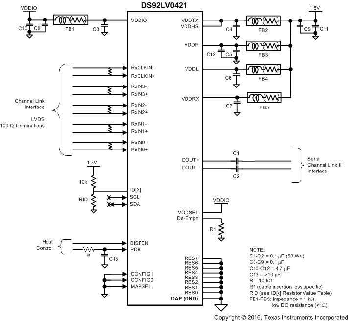 Figure 36. DS92LV0421 Typical Connection Diagram
8.2.1.1 Design Requirements
For this design example, use the parameters listed in Table 16 as the input parameters.
Table 16. Design Parameters
| PARAMETER | VALUE |
|---|---|
| VDDIO | 1.8 V or 3.3 V |
| VDDL, VDDP, VDDHS, VDDTX, VDDRX | 1.8 V |
| AC Coupling Capacitor for DOUT± | 100 nF |
8.2.1.2 Detailed Design Procedure
The DOUT± outputs require 100-nF, AC-coupling capacitors to the line. Channel-Link data input pairs require an external 100-Ω termination for standard LVDS levels. The power supply filter capacitors are placed near the power supply pins. A smaller capacitance capacitor must be placed closer to the power supply pins. Adding a ferrite bead is optional, and if used, TI recommends using a ferrite bead with 1-kΩ impedance and low DC resistance (less than 1 Ω). The VODSEL pin is tied to VDDIO for long cable applications. The de-emphasis pin may connect a resistor to Ground (see Table 2). The PDB and BISTEN pins are assumed to be controlled by a microprocessor. The PDB must remain in a low state until all power supply voltages reach the final voltage. The CONFIG[1:0] pins are set depending on operating modes and backward compatibility (see Table 10). The MAPSEL pin sets the mapping scheme (see Figure 23 and Figure 24). The SCL, SDA, and ID[X] pins can be left open when these serial bus control pins are unused. The RES[7:0] pins and DAP must be tied to Ground.
8.2.1.3 Application Curves
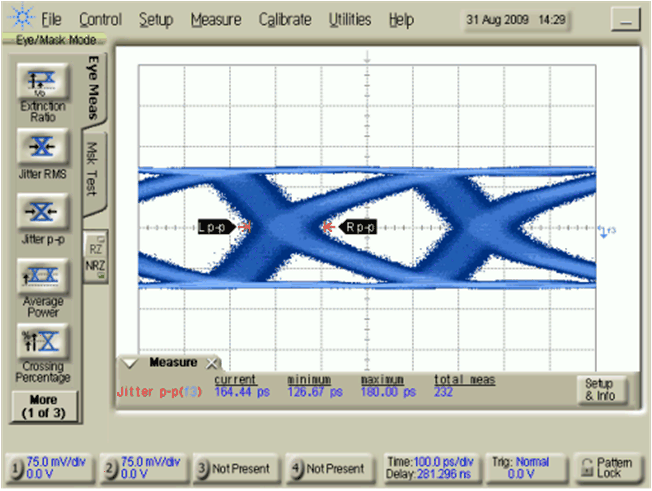
RXCLKIN = 65 MHz, VODSEL = L
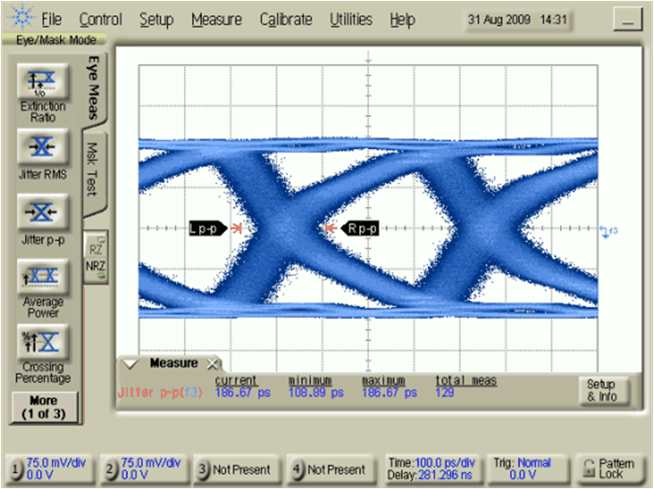
RXCLKIN = 65 MHz, VODSEL = H
8.2.2 DS92LV0422 Typical Application
Figure 39 shows a typical application of the DS92LV0422 for a 24-bit application. The CML inputs require 0.1-µF, AC-coupling capacitors to the line, and the receiver provides internal termination. Bypass capacitors are placed near the power supply pins. At a minimum, four 0.1-µF capacitors and a 4.7-µF capacitor must be used for local device bypassing. Ferrite beads are placed on the power lines for effective noise suppression. System GPO (General Purpose Output) signals control the PDB and BISTEN pins. A delay cap is placed on the PDB signal to delay the enabling of the device until power is stable.
The application assumes connection to the companion serializer (DS92LV0421), and therefore the configuration pins CONFIG[1:0] are also both tied low. The interface to the host is with 1.8-V LVCMOS levels, thus the VDDIO pin is connected also to the 1.8-V rail. The optional serial bus control is not used in this example, thus the SCL, SDA, and ID[X] pins can be left open.
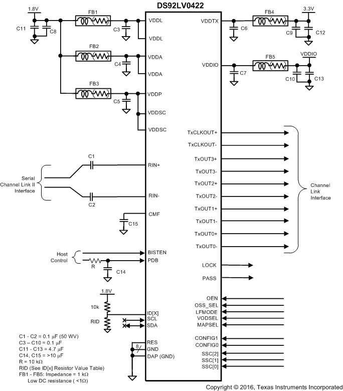 Figure 39. DS92LV0422 Typical Connection Diagram
8.2.2.1 Design Requirements
For this design example, use the parameters listed in Table 17 as the input parameters.
Table 17. Design Parameters
| PARAMETER | VALUE |
|---|---|
| VDDIO | 1.8 V or 3.3 V |
| VDDL, VDDP, VDDSC, VDDA | 1.8 V |
| VDDTX | 3.3 V |
| AC Coupling Capacitor for RIN± | 100 nF |
8.2.2.2 Detailed Design Procedure
The RIN± inputs require 100-nF, AC-coupling capacitors to the line. The power supply filter capacitors are placed near the power supply pins. A smaller capacitance capacitor must be placed closer to the power supply pins. The device has one configuration pin (EQ) called a strap pin, which is pulled down by default. For a high state, use a 10-kΩ resistor pullup to VDDIO. The PDB and BISTEN pins are assumed to be controlled by a microprocessor. The PDB must remain in a low state until all power supply voltages reach the final voltage. The SCL, SDA, and ID[X] pins can be left open when these serial bus control pins are unused. The RES pin and DAP must be tied to Ground.
8.2.2.3 Application Curves
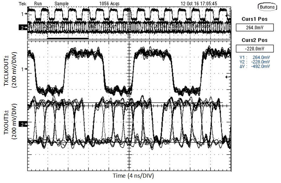 Figure 40. LVDS Parallel Output Data and Clock,
 PRBS-7, TXCLKOUT = 75 MHz, VODSEL = L
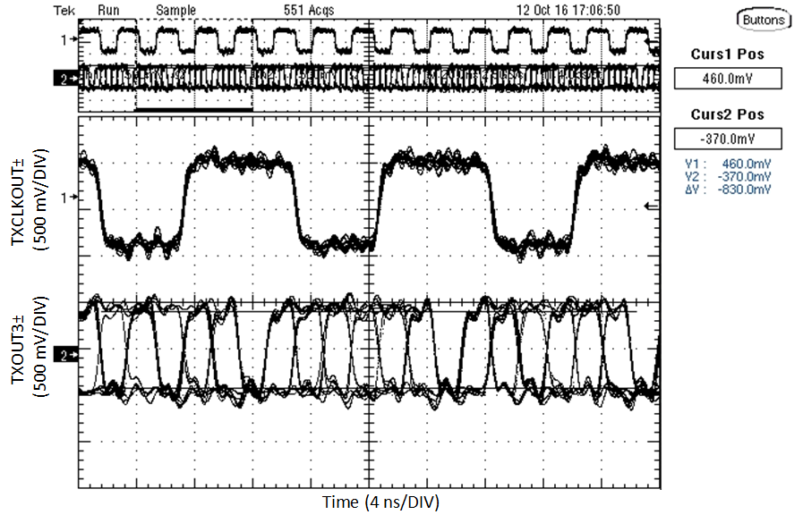 Figure 41. LVDS Parallel Output Data and Clock,
 PRBS-7, TXCLKOUT = 75 MHz, VODSEL = H