SNLS325D May 2010 – December 2016 DS92LV0421 , DS92LV0422
PRODUCTION DATA.
- 1 Features
- 2 Applications
- 3 Description
- 4 Revision History
- 5 Pin Configuration and Functions
-
6 Specifications
- 6.1 Absolute Maximum Ratings
- 6.2 ESD Ratings
- 6.3 Recommended Operating Conditions
- 6.4 Thermal Information
- 6.5 Electrical Characteristics: Serializer DC
- 6.6 Electrical Characteristics: Deserializer DC
- 6.7 Electrical Characteristics: DC and AC Serial Control Bus
- 6.8 Timing Requirements: Serial Control Bus
- 6.9 Switching Characteristics: Serializer
- 6.10 Switching Characteristics: Deserializer
- 6.11 Typical Characteristics
-
7 Detailed Description
- 7.1 Overview
- 7.2 Functional Block Diagrams
- 7.3
Feature Description
- 7.3.1 Parallel LVDS Data Transfer (Color Bit Mapping Select)
- 7.3.2 Serial Data Transfer
- 7.3.3 Video Control Signal Filter
- 7.3.4 Serializer Functional Description
- 7.3.5
Deserializer Functional Description
- 7.3.5.1 Signal Quality Enhancers
- 7.3.5.2 EMI Reduction Features
- 7.3.5.3 Deserializer Clock-Data Recovery Status Flag (LOCK), Output Enable (OEN), and Output State Select (OSS_SEL)
- 7.3.5.4 Deserializer Oscillator Output (Optional)
- 7.3.6 Built-In Self Test (BIST)
- 7.3.7 Optional Serial Bus Control
- 7.4 Device Functional Modes
- 7.5 Register Maps
- 8 Application and Implementation
- 9 Power Supply Recommendations
- 10Layout
- 11Device and Documentation Support
- 12Mechanical, Packaging, and Orderable Information
封装选项
请参考 PDF 数据表获取器件具体的封装图。
机械数据 (封装 | 引脚)
- RHS|48
散热焊盘机械数据 (封装 | 引脚)
- RHS|48
订购信息
6 Specifications
6.1 Absolute Maximum Ratings
over operating free-air temperature range (unless otherwise noted)(1)(2)(3)| MIN | MAX | UNIT | ||
|---|---|---|---|---|
| Supply voltage | VDDn (1.8 V) | –0.3 | 2.5 | V |
| VDDIO | –0.3 | 4 | ||
| Serializer, VDDTX | –0.3 | 2.5 | ||
| Deserializer, VDDTX | –0.3 | 4 | ||
| LVCMOS I/O voltage | –0.3 | VDDIO + 0.3 | V | |
| Serializer LVDS input voltage | –0.3 | VDDIO + 0.3 | V | |
| Deserializer LVDS output voltage | –0.3 | VDDTX + 0.3 | V | |
| Serializer CML driver output voltage | –0.3 | VDDn + 0.3 | V | |
| Deserializer CML receiver input voltage | –0.3 | VDD + 0.3 | V | |
| Junction temperature,TJ | 150 | °C | ||
| Storage temperature, Tstg | –65 | 150 | °C | |
(1) Stresses beyond those listed under Absolute Maximum Ratings may cause permanent damage to the device. These are stress ratings only, which do not imply functional operation of the device at these or any other conditions beyond those indicated under Recommended Operating Conditions. Exposure to absolute-maximum-rated conditions for extended periods may affect device reliability.
(2) If Military/Aerospace specified devices are required, please contact the Texas Instruments Sales Office/Distributors for availability and specifications.
(3) For soldering specifications, see Absolute Maximum Ratings for Soldering (SNOA549).
6.2 ESD Ratings
| VALUE | UNIT | ||||
|---|---|---|---|---|---|
| V(ESD) | Electrostatic discharge | Human-body model (HBM), per ANSI/ESDA/JEDEC JS-001(1) | ±8000 | V | |
| Charged-device model (CDM), per JEDEC specification JESD22-C101(2) | ±1250 | ||||
| Machine Model | ±250 | ||||
| IEC 61000-4-2, powered-up only contact discharge RD = 330 Ω, CS = 150 pF (RIN+, RIN–) |
>±8000 | ||||
| IEC 61000-4-2, powered-up only air-gap discharge RD = 330 Ω, CS = 150 pF (RIN+, RIN–) |
>±30000 | ||||
(1) JEDEC document JEP155 states that 500-V HBM allows safe manufacturing with a standard ESD control process.
(2) JEDEC document JEP157 states that 250-V CDM allows safe manufacturing with a standard ESD control process.
6.3 Recommended Operating Conditions
over operating free-air temperature range (unless otherwise noted)| MIN | NOM | MAX | UNIT | ||
|---|---|---|---|---|---|
| VDDn | Supply voltage | 1.71 | 1.8 | 1.89 | V |
| VDDTX | Supply voltage (serializer) | 1.71 | 1.8 | 1.89 | V |
| VDDTX | Supply voltage (deserializer) | 3 | 3.3 | 3.6 | V |
| VDDIO | LVCMOS supply voltage (1.8-V nominal) | 1.71 | 1.8 | 1.89 | V |
| VDDIO | LVCMOS supply voltage (3.3-V nominal) | 3 | 3.3 | 3.6 | V |
| Clock frequency | 10 | 75 | MHz | ||
| Supply noise(1) | 100 | mVp-p | |||
| TA | Operating free-air temperature | −40 | 25 | 85 | °C |
(1) Supply noise testing was done with minimum capacitors on the PCB. A sinusoidal signal is AC-coupled to the VDDn (1.8 V) supply with amplitude = 100 mVp-p measured at the device VDDn pins. Bit error rate testing of input to the serializer and output of the deserializer with 10 meter cable shows no error when the noise frequency on the serializer is less than 750 kHz. The deserializer, on the other hand, shows no error when the noise frequency is less than 400 kHz.
6.4 Thermal Information
over operating free-air temperature range (unless otherwise noted)| THERMAL METRIC(1) | DS92LV0421 | DS92LV0422 | UNIT | |
|---|---|---|---|---|
| NJK (WQFN) | RHS (WQFN) | |||
| 36 PINS | 48 PINS | |||
| RθJA | Junction-to-ambient thermal resistance(2) | 33.8 | 28.8 | °C/W |
| RθJC(top) | Junction-to-case (top) thermal resistance(2) | 15.8 | 9.3 | °C/W |
| RθJB | Junction-to-board thermal resistance | 7.2 | 5.7 | °C/W |
| ψJT | Junction-to-top characterization parameter | 0.2 | 0.1 | °C/W |
| ψJB | Junction-to-board characterization parameter | 7.1 | 5.7 | °C/W |
| RθJC(bot) | Junction-to-case (bottom) thermal resistance | 2.6 | 1.6 | °C/W |
(1) For more information about traditional and new thermal metrics, see the Semiconductor and IC Package Thermal Metrics application report.
(2) Based on nine thermal vias.
6.5 Electrical Characteristics: Serializer DC
over recommended operating supply and temperature ranges (unless otherwise noted)(1)(2)| PARAMETER | TEST CONDITIONS | MIN | TYP | MAX | UNIT | ||
|---|---|---|---|---|---|---|---|
| LVCMOS INPUT DC SPECIFICATIONS | |||||||
| VIH | High-level input voltage | VDDIO = 3 V to 3.6 V (PDB, VODSEL, MAPSEL, CONFIG[1:0], BISTEN pins) | 2 | VDDIO | V | ||
| VDDIO = 1.71 V to 1.89 V (PDB, VODSEL, MAPSEL, CONFIG[1:0], BISTEN pins) | 0.65 × VDDIO | VDDIO | |||||
| VIL | Low-level input voltage | VDDIO = 3 V to 3.6 V (PDB, VODSEL, MAPSEL, CONFIG[1:0], BISTEN pins) | GND | 0.8 | V | ||
| VDDIO = 1.71 V to 1.89 V (PDB, VODSEL, MAPSEL, CONFIG[1:0], BISTEN pins) | GND | 0.35 × VDDIO | |||||
| IIN | Input current | VIN = 0 V or VDDIO (PDB, VODSEL, MAPSEL, CONFIG[1:0], BISTEN pins) | VDDIO = 3 V to 3.6 V | −15 | ±1 | 15 | µA |
| VDDIO = 1.7 V to 1.89 V | −15 | ±1 | 15 | ||||
| CHANNEL LINK PARALLEL LVDS RECEIVER DC SPECIFICATIONS | |||||||
| VTH | Differential threshold, high voltage | VCM = 1.2 V (see Figure 1), RXIN[3:0]± and RXCLKIN± pins |
100 | mV | |||
| VTL | Differential threshold, low voltage | VCM = 1.2 V (see Figure 1), RXIN[3:0]± and RXCLKIN± pins |
−100 | mV | |||
| |VID| | Differential input voltage swing | VCM = 1.2 V (see Figure 1), RXIN[3:0]± and RXCLKIN± pins |
200 | 600 | mV | ||
| VCM | Common-mode voltage | VDDIO = 3.3 V (RXIN[3:0]± and RXCLKIN± pins) | 0 | 1.2 | 2.4 | V | |
| VDDIO = 1.8 V (RXIN[3:0]± and RXCLKIN± pins) | 0 | 1.2 | 1.7 | ||||
| IIN | Input current | RXIN[3:0]± and RXCLKIN± pins | −15 | ±1 | 15 | µA | |
| CHANNEL LINK II SERIAL CML DRIVER DC SPECIFICATIONS | |||||||
| VOD | Differential output voltage | RL = 100 Ω, de-emphasis = disabled (see Figure 3), DOUT+ and DOUT– pins |
VODSEL = L | ±225 | ±300 | ±375 | mV |
| VODSEL = H | ±350 | ±450 | ±550 | ||||
| VODp-p | Differential output voltage (DOUT+) – (DOUT–) |
RL = 100 Ω, de-emphasis = disabled (see Figure 3), DOUT+ and DOUT– pins |
VODSEL = L | 600 | mVp-p | ||
| VODSEL = H | 900 | ||||||
| ΔVOD | Output voltage unbalance | RL = 100 Ω, de-emphasis = disabled, VODSEL = L (DOUT+ and DOUT– pins) | 1 | 50 | mV | ||
| VOS | Offset voltage (single-ended) |
At TP A and B (see Figure 2), RL = 100 Ω, de-emphasis = disabled (DOUT+ and DOUT– pins) | VODSEL = L | 1.65 | V | ||
| VODSEL = H | 1.575 | ||||||
| ΔVOS | Offset voltage unbalance (single-ended) |
At TP A and B (see Figure 2), RL = 100 Ω, de-emphasis = disabled (DOUT+ and DOUT– pins) |
1 | mV | |||
| IOS | Output short-circuit current | DOUT± = 0 V, de-emphasis = disabled, VODSEL = 0 (DOUT+ and DOUT– pins) |
−36 | mA | |||
| RTO | Internal output termination resistor | DOUT+ and DOUT– pins | 80 | 120 | Ω | ||
| SERIALIZER SUPPLY CURRENT | |||||||
| IDDT1 | Serializer supply current (includes load current) |
RL = 100 Ω, f = 75 MHz, checker board pattern (see Figure 15), de-emphasis = 3 kΩ, VODSEL = H, VDD = 1.89 V (All VDD pins) |
84 | 100 | mA | ||
| IDDIOT1 | Serializer supply current (includes load current) |
RL = 100 Ω, f = 75 MHz de-emphasis = 3 kΩ, VODSEL = H, checker board pattern (see Figure 15) |
VDDIO= 1.89 V (VDDIO pin) | 3 | 5 | mA | |
| VDDIO = 3.6 V (VDDIO pin) | 10 | 13 | |||||
| IDDT2 | Serializer supply current (includes load current) |
RL = 100 Ω, f = 75 MHz, checker board pattern (see Figure 15), de-emphasis = 6 kΩ, VODSEL = L, VDD = 1.89 V (All VDD pins) |
77 | 90 | mA | ||
| IDDIOT2 | Serializer supply current (includes load current) |
RL = 100 Ω, f = 75 MHz de-emphasis = 6 kΩ, VODSEL = L, checker board pattern (see Figure 15) |
VDDIO= 1.89 V (VDDIO pin) | 3 | 5 | mA | |
| VDDIO = 3.6 V (VDDIO pin) | 10 | 13 | |||||
| IDDZ | Serializer supply current power-down | PDB = 0 V, all other LVCMOS inputs = 0 V, VDD = 1.89 V (All VDD pins) |
100 | 1000 | µA | ||
| IDDIOZ | Serializer supply current power-down | PDB = 0 V, all other LVCMOS inputs = 0 V | VDDIO= 1.89 V (VDDIO pin) | 0.5 | 10 | µA | |
| VDDIO = 3.6 V (VDDIO pin) | 1 | 30 | |||||
(1) Typical values represent most likely parametric norms at VDD = 3.3 V, TA = +25°C, and at the Recommended Operation Conditions at the time of product characterization and are not verified.
(2) Current into device pins is defined as positive. Current out of a device pin is defined as negative. Voltages are referenced to ground except VOD, ΔVOD, VTH, and VTL, which are differential voltages.
6.6 Electrical Characteristics: Deserializer DC
over recommended operating supply and temperature ranges (unless otherwise noted)(1)(2)| PARAMETER | TEST CONDITIONS | MIN | TYP | MAX | UNIT | ||
|---|---|---|---|---|---|---|---|
| 3.3-V LVCMOS I/O DC SPECIFICATIONS (VDDIO = 3 V to 3.6 V) | |||||||
| VIH | High level input voltage | PDB, VODSEL, OEN, MAPSEL, LFMODE, SSC[2:0], and BISTEN pins | 2 | VDDIO | V | ||
| VIL | Low level input voltage | PDB, VODSEL, OEN, MAPSEL, LFMODE, SSC[2:0], and BISTEN pins | GND | 0.8 | V | ||
| IIN | Input current | VIN = 0 V or VDDIO (PDB, VODSEL, OEN, MAPSEL, LFMODE, SSC[2:0], and BISTEN pins) | −15 | ±1 | 15 | µA | |
| VOH | High level output voltage | IOH = –0.5 mA (LOCK and PASS pins) | VDDIO – 0.2 | VDDIO | V | ||
| VOL | Low level output voltage | IOL = 0.5 mA (LOCK and PASS pins) | GND | 0.2 | V | ||
| IOS | Output short-circuit current | VOUT = 0 V (LOCK and PASS pins) | –10 | mA | |||
| IOZ | TRI-STATE output current | PDB = 0 V, OSS_SEL = 0 V, VOUT = 0 V or VDDIO (LOCK and PASS pins) | –10 | 10 | µA | ||
| 1.8-V LVCMOS I/O DC SPECIFICATIONS (VDDIO = 1.71 V to 1.89 V) | |||||||
| VIH | High level input voltage | PDB, VODSEL, OEN, MAPSEL, LFMODE, SSC[2:0], and BISTEN pins | 0.65 × VDDIO | VDDIO | V | ||
| VIL | Low level input voltage | PDB, VODSEL, OEN, MAPSEL, LFMODE, SSC[2:0], and BISTEN pins | GND | 0.35 × VDDIO | V | ||
| IIN | Input current | VIN = 0 V or VDDIO (PDB, VODSEL, OEN, MAPSEL, LFMODE, SSC[2:0], and BISTEN pins) | −15 | ±1 | 15 | µA | |
| VOH | High level output voltage | IOH = –0.5 mA (LOCK and PASS pins) | VDDIO – 0.2 | VDDIO | V | ||
| VOL | Low level output voltage | IOL = 0.5 mA (LOCK and PASS pins) | GND | 0.2 | V | ||
| IOS | Output short-circuit current | VOUT = 0 V (LOCK and PASS pins) | –3 | mA | |||
| IOZ | TRI-STATE output current | PDB = 0 V, OSS_SEL = 0 V, VOUT = 0 V or VDDIO (LOCK and PASS pins) | –15 | 15 | µA | ||
| CHANNEL LINK PARALLEL LVDS DRIVER DC SPECIFICATIONS | |||||||
| |VOD| | Differential output voltage | RL = 100 Ω (see Figure 3; TXOUT[3:0]± and TXCLKOUT± pins) |
VODSEL = L | 100 | 250 | 400 | mV |
| VODSEL = H | 200 | 400 | 600 | ||||
| VODp-p | Differential output voltage A to B |
RL = 100 Ω (see Figure 3; TXOUT[3:0]± and TXCLKOUT± pins) |
VODSEL = L | 500 | mVp-p | ||
| VODSEL = H | 800 | ||||||
| ΔVOD | Output voltage unbalance | RL = 100 Ω (see Figure 3; TXOUT[3:0]± and TXCLKOUT± pins) |
1 | 50 | mV | ||
| VOS | Offset voltage (single-ended) |
RL = 100 Ω (see Figure 3; TXOUT[3:0]± and TXCLKOUT± pins) |
VODSEL = L | 1 | 1.2 | 1.5 | V |
| VODSEL = H | 1.2 | ||||||
| ΔVOS | Offset voltage unbalance (single-ended) |
RL = 100 Ω (see Figure 3; TXOUT[3:0]± and TXCLKOUT± pins) | 1 | 50 | mV | ||
| IOS | Output short-circuit current | RL = 100 Ω, VOUT = GND (TXOUT[3:0]± and TXCLKOUT± pins) |
–5 | mA | |||
| IOZ | Output TRI-STATE current | RL = 100 Ω, VOUT = VDDTX or GND (TXOUT[3:0]± and TXCLKOUT± pins) |
–10 | 10 | µA | ||
| CHANNEL LINK II SERIAL CML RECEIVER DC SPECIFICATIONS | |||||||
| VTH | Differential input threshold high voltage | VCM = 1.2 V (Internal VBIAS) (RIN+ and RIN- pins) |
50 | mV | |||
| VTL | Differential input threshold low voltage | VCM = 1.2 V (Internal VBIAS) (RIN+ and RIN- pins) |
–50 | mV | |||
| VCM | Common mode voltage, internal VBIAS | RIN+ and RIN- pins | 1.2 | V | |||
| RT | Input termination | RIN+ and RIN- pins | 85 | 100 | 115 | Ω | |
| DESERIALIZER SUPPLY CURRENT | |||||||
| IDD1 | Deserializer supply current (Includes load current) |
75 MHz clock, checker board pattern (see Figure 15), VODSEL = H, SSCG[2:0] = 000'b, VDDn = 1.89 V (All VDD(1.8) pins) |
88 | 100 | mA | ||
| IDDTX1 | Deserializer supply current (Includes load current) |
75 MHz clock, checker board pattern (see Figure 15), VODSEL = H, SSCG[2:0] = 000'b, VDDTX = 3.6 V (VDDTX pin) |
40 | 50 | mA | ||
| IDDIO1 | Deserializer supply current (Includes load current) |
75 MHz clock, checker board pattern (see Figure 15), VODSEL = H, SSCG[2:0] = 000'b |
VDDIO = 1.89 V (VDDIO pin) | 0.3 | 0.8 | mA | |
| VDDIO = 3.6 V (VDDIO pin) | 0.8 | 1.5 | |||||
| IDDZ | Deserializer supply current power-down | PDB = 0 V, All other LVCMOS inputs = 0 V, VDDn = 1.89 V (All VDD(1.8) pins) |
0.15 | 2 | mA | ||
| IDDTXZ | Deserializer supply current power-down | PDB = 0 V, All other LVCMOS inputs = 0 V, VDDTX = 3.6 V (VDDTX pin) |
0.01 | 0.1 | mA | ||
| IDDIOZ | Deserializer supply current power-down | PDB = 0 V, all other LVCMOS inputs = 0 V |
VDDIO = 1.89 V (VDDIO pin) | 0.01 | 0.08 | mA | |
| VDDIO = 3.6 V (VDDIO pin) | 0.01 | 0.08 | |||||
(1) Typical values represent most likely parametric norms at VDD = 3.3 V, TA = +25°C, and at the Recommended Operation Conditions at the time of product characterization and are not verified.
(2) Current into device pins is defined as positive. Current out of a device pin is defined as negative. Voltages are referenced to ground except VOD, ΔVOD, VTH, and VTL, which are differential voltages.
6.7 Electrical Characteristics: DC and AC Serial Control Bus
over 3.3-V supply and temperature ranges (unless otherwise noted)| PARAMETER | TEST CONDITIONS | MIN | TYP | MAX | UNIT | |
|---|---|---|---|---|---|---|
| VIH | Input high-level voltage | SDA and SCL | 0.7 × VDDIO | VDDIO | V | |
| VIL | Input low-level voltage | SDA and SCL | GND | 0.3 × VDDIO | V | |
| VHY | Input hysteresis | >50 | mV | |||
| VOL | Output low-level voltage | SDA, IOL = 0.5 mA | 0 | 0.36 | V | |
| IIN | Input current | SDA or SCL, Vin = VDDIO or GND | –10 | 10 | µA | |
| tR | SDA rise time, READ | SDA, RPU = 10 kΩ, Cb ≤ 400pF (see Figure 18) |
800 | ns | ||
| tF | SDA fall time, READ | SDA, RPU = 10 kΩ, Cb ≤ 400pF (see Figure 18) |
50 | ns | ||
| tSU;DAT | Set-up time, READ | See Figure 18 | 540 | ns | ||
| tHD;DAT | Hold time, READ | See Figure 18 | 600 | ns | ||
| tSP | Input filter | 50 | ns | |||
| CIN | Input capacitance | SDA or SCL | <5 | pF | ||
6.8 Timing Requirements: Serial Control Bus
over 3.3-V supply and temperature ranges (unless otherwise noted)| MIN | TYP | MAX | UNIT | |||
|---|---|---|---|---|---|---|
| fSCL | SCL clock frequency | Standard mode | 100 | kHz | ||
| Fast mode | 400 | |||||
| tLOW | SCL low period | Standard mode | 4.7 | µs | ||
| Fast mode | 1.3 | |||||
| tHIGH | SCL high period | Standard mode | 4 | µs | ||
| Fast mode | 0.6 | |||||
| tHD:STA | Hold time for a START or a repeated START condition (see Figure 18) | Standard mode | 4 | µs | ||
| Fast mode | 0.6 | |||||
| tSU:STA | Set-up time for a START or a repeated START condition (see Figure 18) | Standard mode | 4.7 | µs | ||
| Fast mode | 0.6 | |||||
| tHD:DAT | Data hold time (see Figure 18) | Standard mode | 0 | 3.45 | µs | |
| Fast mode | 0 | 0.9 | ||||
| tSU:DAT | Data set-up time (see Figure 18) | Standard mode | 250 | µs | ||
| Fast mode | 100 | |||||
| tSU:STO | Set-up time for STOP (see Figure 18) | Standard mode | 4 | µs | ||
| Fast mode | 0.6 | |||||
| tBUF | Bus free time between STOP and START (see Figure 18) |
Standard mode | 4.7 | µs | ||
| Fast mode | 1.3 | |||||
| tr | SCL and SDA rise time (see Figure 18) | Standard mode | 1000 | ns | ||
| Fast mode | 300 | |||||
| tf | SCL and SDA fall time (see Figure 18) | Standard mode | 300 | ns | ||
| Fast mode | 300 | |||||
6.9 Switching Characteristics: Serializer
over recommended operating supply and temperature range (unless otherwise noted)| PARAMETER | TEST CONDITIONS | MIN | TYP | MAX | UNIT | |
|---|---|---|---|---|---|---|
| CHANNEL LINK PARALLEL LVDS INPUT | ||||||
| tRSP0 | LVDS Receiver Strobe Position (bit 0) | RXCLKIN = 75 MHz, RXIN[3:0] pins (see Figure 5) |
0.57 | 0.95 | 1.33 | ns |
| tRSP1 | LVDS Receiver Strobe Position (bit 1) | RXCLKIN = 75 MHz, RXIN[3:0] pins (see Figure 5) |
2.47 | 2.85 | 3.23 | ns |
| tRSP2 | LVDS Receiver Strobe Position (bit 2) | RXCLKIN = 75 MHz, RXIN[3:0] pins (see Figure 5) |
4.37 | 4.75 | 5.13 | ns |
| tRSP3 | LVDS Receiver Strobe Position (bit 3) | RXCLKIN = 75 MHz, RXIN[3:0] pins (see Figure 5) |
6.27 | 6.65 | 7.03 | ns |
| tRSP4 | LVDS Receiver Strobe Position (bit 4) | RXCLKIN = 75 MHz, RXIN[3:0] pins (see Figure 5) |
8.17 | 8.55 | 8.93 | ns |
| tRSP5 | LVDS Receiver Strobe Position (bit 5) | RXCLKIN = 75 MHz, RXIN[3:0] pins (see Figure 5) |
10.07 | 10.45 | 10.83 | ns |
| tRSP6 | LVDS Receiver Strobe Position (bit 6) | RXCLKIN = 75 MHz, RXIN[3:0] pins (see Figure 5) |
11.97 | 12.35 | 12.73 | ns |
| CHANNEL LINK II CML OUTPUT | ||||||
| tLLHT | Serializer output low-to-high transition time (see Figure 4) |
RL = 100 Ω, De-emphasis = disabled, VODSEL = 0 |
100 | 200 | 300 | ps |
| RL = 100 Ω, De-emphasis = disabled, VODSEL = 1 |
100 | 200 | 300 | |||
| tLHLT | Serializer output high-to-low transition time (see Figure 4) |
RL = 100 Ω, De-emphasis = disabled, VODSEL = 0 |
130 | 260 | 390 | ps |
| RL = 100 Ω, De-emphasis = disabled, VODSEL = 1 |
100 | 200 | 300 | |||
| tXZD | Serializer output active to OFF delay (see Figure 9)(1) |
5 | 15 | ns | ||
| tPLD | Serializer PLL lock time (see Figure 7)(1)(2)(3) |
RL = 100 Ω | 1.5 | 10 | ms | |
| tSD | Serializer delay, latency (see Figure 10)(1) |
RL = 100 Ω | 147 × T | 148 × T | ns | |
| tDJIT | Serializer output total jitter (see Figure 12) |
RL = 100 Ω, De-emphasis = disabled, RANDOM pattern |
0.3 | UI(4) | ||
| λSTXBW | Serializer jitter transfer (function –3-dB bandwidth)(1)(5) |
RXCLKIN = 43 MHz | 2.2 | MHz | ||
| RXCLKIN = 75 MHz | 3 | |||||
| δSTX | Serializer jitter transfer (function peaking)(1)(5) |
RXCLKIN = 43 MHz | 1 | dB | ||
| RXCLKIN = 75 MHz | 1 | |||||
(1) Specification is verified by characterization and is not tested in production.
(2) tPLD and tDDLT is the time required by the serializer and deserializer to obtain lock when exiting power-down state with an active RXCLKIN.
(3) When the serializer output is at TRI-STATE, the deserializer loses PLL lock. Resynchronization and Re-lock must occur before data transfer require tPLD.
(4) UI: Unit Interval is equivalent to one serialized data bit width (1 UI = 1 / [28 × CLK]). The UI scales with clock frequency.
(5) Specification is verified by design and is not tested in production.
6.10 Switching Characteristics: Deserializer
over recommended operating supply and temperature range (unless otherwise noted)| PARAMETER | TEST CONDITIONS | MIN | TYP | MAX | UNIT | |
|---|---|---|---|---|---|---|
| CHANNEL LINK PARALLEL LVDS OUTPUT | ||||||
| tDLHT | Deserializer low-to-high transition time | RL = 100 Ω TXCLKOUT±, TXOUT[3:0]± pins |
0.3 | 0.6 | ns | |
| tDHLT | Deserializer high-to-low transition time | RL = 100 Ω TXCLKOUT±, TXOUT[3:0]± pins |
0.3 | 0.6 | ns | |
| tDCCJ | Cycle-to-cycle output jitter(1)(2)(3) | TXCLKOUT± = 10 MHz | 900 | 2100 | ps | |
| TXCLKOUT± = 75 MHz | 75 | 125 | ||||
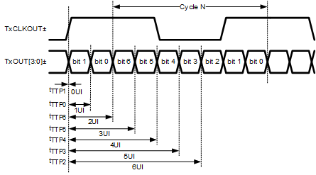
| tTTP1 | LVDS Transmitter Pulse Position for bit 1 | TXCLKOUT± = 10 to 75 MHz (see Figure 6) |
0 | UI(4) | ||
| tTTP0 | LVDS Transmitter Pulse Position for bit 0 | TXCLKOUT± = 10 to 75 MHz (see Figure 6) |
1 | UI(4) | ||
| tTTP6 | LVDS Transmitter Pulse Position for bit 6 | TXCLKOUT± = 10 to 75 MHz (see Figure 6) |
2 | UI(4) | ||
| tTTP5 | LVDS Transmitter Pulse Position for bit 5 | TXCLKOUT± = 10 to 75 MHz (see Figure 6) |
3 | UI(4) | ||
| tTTP4 | LVDS Transmitter Pulse Position for bit 4 | TXCLKOUT± = 10 to 75 MHz (see Figure 6) |
4 | UI(4) | ||
| tTTP3 | LVDS Transmitter Pulse Position for bit 3 | TXCLKOUT± = 10 to 75 MHz (see Figure 6) |
5 | UI(4) | ||
| tTTP2 | LVDS Transmitter Pulse Position for bit 2 | TXCLKOUT± = 10 to 75 MHz (see Figure 6) |
6 | UI(4) | ||
| tDD | Deserializer delay, latency(3)
(see Figure 11) |
TXCLKOUT± = 10 to 75 MHz (see Figure 6) |
142 × T | 143 × T | ns | |
| tTPDD | Deserializer power-down delay, active to OFF (see Figure 13) |
TXCLKOUT± = 75 MHz | 6 | 10 | ns | |
| tTXZR | Deserializer enable delay, OFF to active (see Figure 14) |
TXCLKOUT± = 75 MHz | 40 | 55 | ns | |
| CHANNEL LINK II CML INPUT | ||||||
| tDDLT | Deserializer lock time(5)
(see Figure 8) |
TXCLKOUT± = 10 MHz, SSCG = OFF | 7 | ms | ||
| TXCLKOUT± = 10 MHz, SSCG = ON | 14 | |||||
| TXCLKOUT± = 75 MHz, SSCG = OFF | 6 | |||||
| TXCLKOUT± = 65 MHz, SSCG = ON | 8 | |||||
| tDJIT | Deserializer input jitter tolerance (see Figure 16) |
EQ = OFF SSCG = OFF Jitter frequency > 10 MHz |
>0.45 | UI(6) | ||
| LVCMOS OUTPUTS | ||||||
| tCLH | Deserializer low-to-high transition time (see Figure 4) |
CL = 8 pF (LOCK and PASS pins) | 10 | 15 | ns | |
| tCHL | Deserializer high-to-low transition time (see Figure 4) |
CL = 8 pF (LOCK and PASS pins) | 10 | 15 | ns | |
| tPASS | BIST PASS valid time, BISTEN = 1 (see Figure 17) |
10 MHz (PASS pin) |
220 | 230 | ns | |
| 75 MHz (PASS pin) |
40 | 65 | ||||
| SSCG MODE | ||||||
| fDEV | Spread spectrum clocking deviation frequency(3) |
TXCLKOUT± = 10 to 65 MHz, SSCG = ON |
±0.5% | ±2% | ||
| fMOD | Spread spectrum clocking modulation frequency(3) |
TXCLKOUT± = 10 to 65 MHz, SSCG = ON |
8 | 100 | kHz | |
(1) tDCCJ is the maximum amount of jitter between adjacent clock cycles.
(2) Specification is verified by characterization and is not tested in production.
(4) UI: Unit Interval is equivalent to one serialized data bit width in the OpenLDI parallel interface format (1 UI = 1 / [7 × CLK]). The UI scales with clock frequency.
(5) tPLD and tDDLT is the time required by the serializer and deserializer to obtain lock when exiting power-down state with an active RXCLKIN.
(6) UI – Unit Interval is equivalent to one serialized data bit width (1 UI = 1 / [28 × CLK]). The UI scales with clock frequency.
 Figure 1. Channel Link DC VTH/VTL Definition
 Figure 2. Output Test Circuit
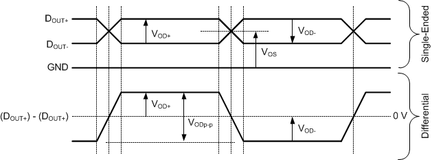 Figure 3. CML Output Waveforms
 Figure 4. CML Output Transition Times
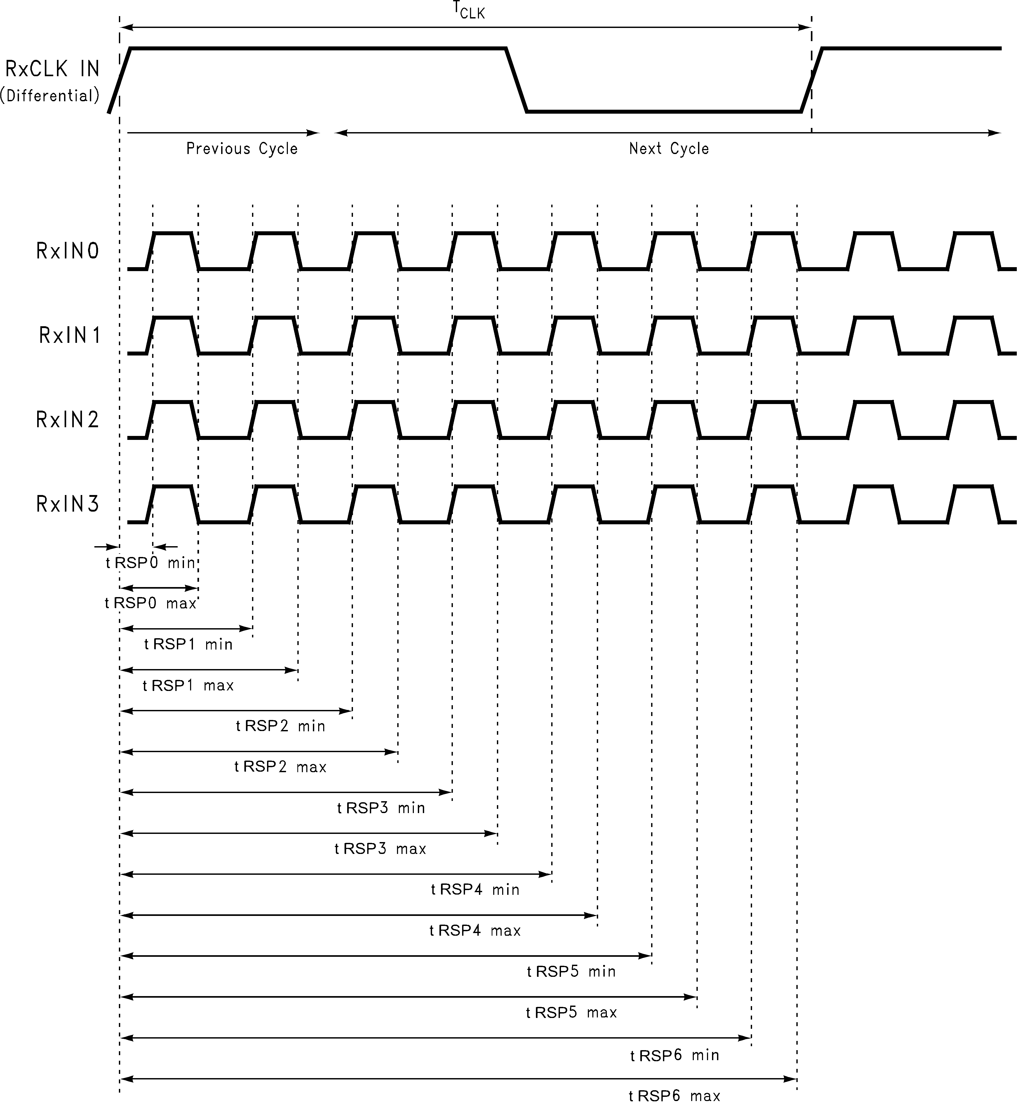 Figure 5. DS92LV0421 Channel Link Receiver Strobe Positions
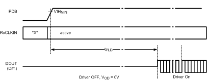 Figure 7. DS92LV0421 Lock Time
 Figure 8. DS92LV0422 Lock Time
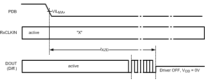 Figure 9. DS92LV0421 Disable Time
 Figure 10. DS92LV0421 Latency Delay
 Figure 11. DS92LV0422 Latency Delay
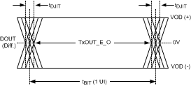 Figure 12. DS92LV0421 Output Jitter
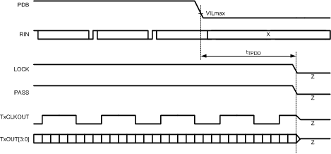 Figure 13. DS92LV0422 Power-Down Delay
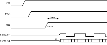 Figure 14. DS92LV0422 Enable Delay
 Figure 15. Checkerboard Data Pattern
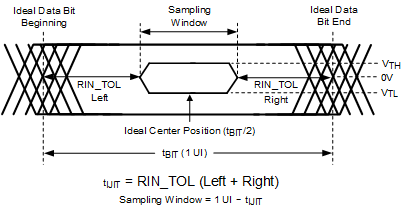 Figure 16. DS92LV0422 Receiver Input Jitter Tolerance
 Figure 17. BIST PASS Waveform
 Figure 18. Serial Control Bus Timing Diagram
6.11 Typical Characteristics
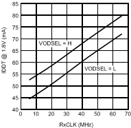 Figure 19. Typical IDDT (1.8-V Supply)
 vs RXCLKIN
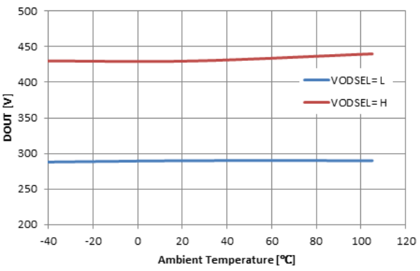 Figure 20. Serializer DOUT Voltage
vs Ambient Temperature
