ZHCSGK5B July   2017  – August 2024 ESD401

PRODUCTION DATA  

  1.   1
  2. 特性
  3. 应用
  4. 说明
  5. Pin Configuration and Functions
  6. Specifications
    1. 5.1 Absolute Maximum Ratings
    2. 5.2 ESD Ratings — JEDEC Specification 
    3. 5.3 ESD Ratings—IEC Specification
    4. 5.4 Recommended Operating Conditions
    5. 5.5 Thermal Information
    6. 5.6 Electrical Characteristics
    7. 5.7 Typical Characteristics
  7. Detailed Description
    1. 6.1 Overview
    2. 6.2 Functional Block Diagram
    3. 6.3 Feature Description
      1. 6.3.1 IEC 61000-4-2 ESD Protection
      2. 6.3.2 IEC 61000-4-4 EFT Protection
      3. 6.3.3 IEC 61000-4-5 Surge Protection
      4. 6.3.4 IO Capacitance
      5. 6.3.5 DC Breakdown Voltage
      6. 6.3.6 Low Leakage Current
      7. 6.3.7 Low ESD Clamping Voltage
      8. 6.3.8 Industrial Temperature Range
      9. 6.3.9 Industry Standard Footprint
    4. 6.4 Device Functional Modes
  8. Application and Implementation
    1. 7.1 Application Information
    2. 7.2 Typical Application
      1. 7.2.1 Design Requirements
      2. 7.2.2 Detailed Design Procedure
        1. 7.2.2.1 Signal Range
        2. 7.2.2.2 Operating Frequency
      3. 7.2.3 Application Curves
    3. 7.3 Power Supply Recommendations
    4. 7.4 Layout
      1. 7.4.1 Layout Guidelines
      2. 7.4.2 Layout Example
  9. Device and Documentation Support
    1. 8.1 接收文档更新通知
    2. 8.2 支持资源
    3. 8.3 Trademarks
    4. 8.4 静电放电警告
    5. 8.5 术语表
  10. Revision History
  11. 10Mechanical, Packaging, and Orderable Information
    1. 10.1 Tape and Reel Information
  12. 11Mechanical Data

封装选项

机械数据 (封装 | 引脚)
散热焊盘机械数据 (封装 | 引脚)
订购信息

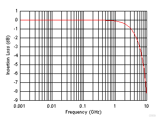
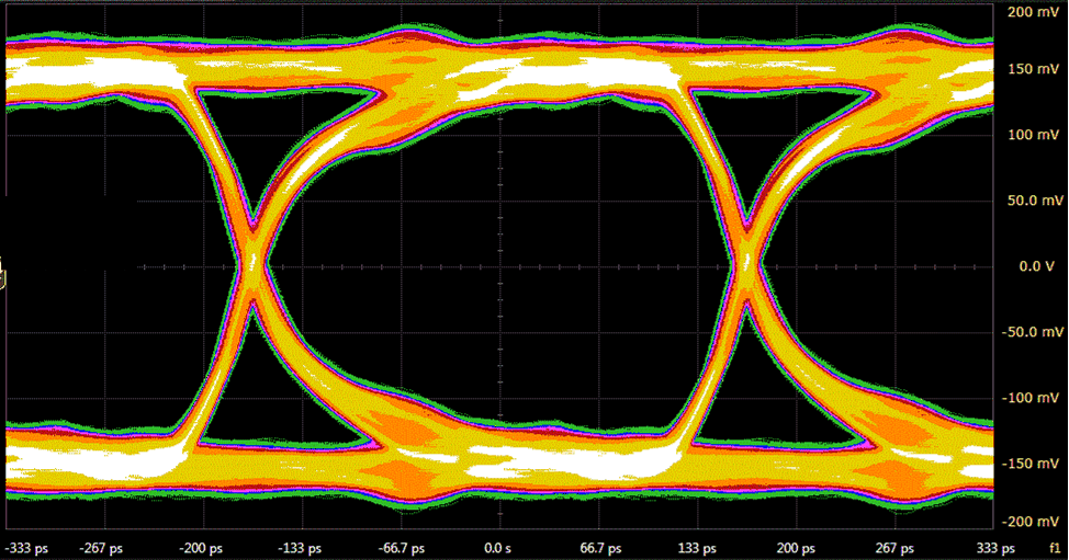
Application Curves

ESD401 Insertion LossFigure 7-2 Insertion Loss
ESD401 Eye Diagram - 3-Gbps Signal No DeviceFigure 7-3 Eye Diagram - 3-Gbps Signal No Device
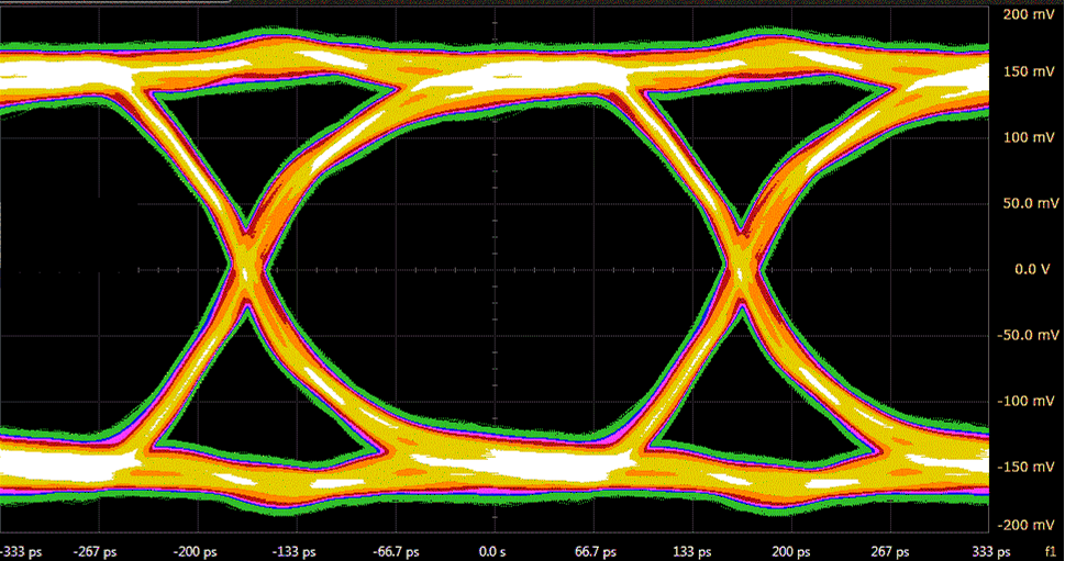
ESD401 Eye Diagram - 3-Gbps Signal With ESD401Figure 7-4 Eye Diagram - 3-Gbps Signal With ESD401