ZHCSBK0D October 2012 – October 2015 F28M36H33B2 , F28M36H53B2 , F28M36P53C2 , F28M36P63C2
PRODUCTION DATA.
- 1器件概述
- 2修订历史记录
- 3Device Comparison
- 4Terminal Configuration and Functions
-
5Specifications
- 5.1 Absolute Maximum Ratings
- 5.2 ESD Ratings
- 5.3 Recommended Operating Conditions
- 5.4 Electrical Characteristics
- 5.5 Power Consumption Summary
- 5.6 Thermal Resistance Characteristics for ZWT Package (Revision 0 Silicon)
- 5.7 Thermal Resistance Characteristics for ZWT Package (Revision A Silicon)
- 5.8 Thermal Design Considerations
- 5.9 Timing and Switching Characteristics
- 5.10
Analog and Shared Peripherals
- 5.10.1 Analog-to-Digital Converter
- 5.10.2 Comparator + DAC Units
- 5.10.3 Interprocessor Communications
- 5.10.4 External Peripheral Interface
- 5.11 Master Subsystem Peripherals
- 5.12
Control Subsystem Peripherals
- 5.12.1 High-Resolution PWM and Enhanced PWM Modules
- 5.12.2 Enhanced Capture Module
- 5.12.3 Enhanced Quadrature Encoder Pulse Module
- 5.12.4 C28x Inter-Integrated Circuit Module
- 5.12.5 C28x Serial Communications Interface
- 5.12.6 C28x Serial Peripheral Interface
- 5.12.7 C28x Multichannel Buffered Serial Port
-
6Detailed Description
- 6.1 Memory Maps
- 6.2 Identification
- 6.3 Master Subsystem
- 6.4 Control Subsystem
- 6.5 Analog Subsystem
- 6.6 Master Subsystem NMIs
- 6.7 Control Subsystem NMIs
- 6.8 Resets
- 6.9 Internal Voltage Regulation and Power-On-Reset Functionality
- 6.10 Input Clocks and PLLs
- 6.11 Master Subsystem Clocking
- 6.12 Control Subsystem Clocking
- 6.13 Analog Subsystem Clocking
- 6.14 Shared Resources Clocking
- 6.15 Loss of Input Clock (NMI Watchdog Function)
- 6.16 GPIOs and Other Pins
- 6.17 Emulation/JTAG
- 6.18 Code Security Module
- 6.19 µCRC Module
- 7Applications, Implementation, and Layout
- 8器件和文档支持
- 9机械、封装和可订购信息
5 Specifications
5.1 Absolute Maximum Ratings(1)(2)
over operating free-air temperature range (unless otherwise noted)| MIN | MAX | UNIT | ||
|---|---|---|---|---|
| Supply voltage | VDDIO (I/O and Flash) with respect to VSS | –0.3 | 4.6 | V |
| VDD18 with respect to VSS | –0.3 | 2.5 | ||
| VDD12 with respect to VSS | –0.3 | 1.5 | ||
| Analog voltage | VDDA with respect to VSSA | –0.3 | 4.6 | V |
| Input voltage | VIN (3.3 V) | –0.3 | 4.6 | V |
| Output voltage | VO | –0.3 | 4.6 | V |
| Supply ramp rate | VDDIO, VDD18, VDD12, VDDA with respect to VSS | 105 | V/s | |
| Input clamp current | IIK (VIN < 0 or VIN > VDDIO)(3) | –20 | 20 | mA |
| Output clamp current | IOK (VO < 0 or VO > VDDIO) | –20 | 20 | mA |
| Free-Air temperature | TA | –40 | 125 | °C |
| Junction temperature(4) | TJ | –40 | 150 | °C |
| Storage temperature(4) | Tstg | –65 | 150 | °C |
5.2 ESD Ratings
| VALUE | UNIT | ||||
|---|---|---|---|---|---|
| F28M36x in 289-ball ZWT package | |||||
| V(ESD) | Electrostatic discharge | Human body model (HBM), per AEC Q100-002(1) | All pins | ±2000 | V |
| Charged device model (CDM), per AEC Q100-011 |
All pins | ±500 | |||
| Corner balls on 289-ball ZWT: A1, A19, W1, W19 |
±750 | ||||
5.3 Recommended Operating Conditions
| MIN | NOM | MAX | UNIT | ||
|---|---|---|---|---|---|
| Device supply voltage, I/O, VDDIO(1) | 2.97 | 3.3 | 3.63 | V | |
| Device supply voltage, Analog Subsystem, VDD18
(when internal VREG is disabled and 1.8 V is supplied externally) |
1.71 | 1.8 | 1.995 | V | |
| Device supply voltage, Master and Control Subsystems, VDD12
(when internal VREG is disabled and 1.2 V is supplied externally) |
1.14 | 1.2 | 1.32 | V | |
| Supply ground, VSS | 0 | V | |||
| Analog supply voltage, VDDA(1) | 2.97 | 3.3 | 3.63 | V | |
| Analog ground, VSSA | 0 | V | |||
| Device clock frequency (system clock) Master Subsystem |
P63C2, P53C2 | 2 | 125 | MHz | |
| H53C2, H53B2, H33C2, H33B2 | 2 | 100 | |||
| Device clock frequency (system clock) Control Subsystem |
2 | 150 | MHz | ||
| Junction temperature, TJ | T version | –40 | 105 | °C | |
| S version(2) | –40 | 125 | |||
| Q version (Q100 qualification)(2) | –40 | 150 | |||
| Free-Air temperature, TA | Q version (Q100 qualification) | –40 | 125 | °C |
5.4 Electrical Characteristics
over recommended operating conditions (unless otherwise noted)| PARAMETER | TEST CONDITIONS | MIN | TYP | MAX | UNIT | ||||
|---|---|---|---|---|---|---|---|---|---|
| VIL | Low-level input voltage (3.3 V) | VSS – 0.3 | VDDIO * 0.3 | V | |||||
| VIH | High-level input voltage (3.3 V) | VDDIO * 0.7 | VDDIO + 0.3 | V | |||||
| VOL | Low-level output voltage | IOL = IOL MAX | VDDIO * 0.2 | V | |||||
| VOH | High-level output voltage | IOH = IOH MAX | VDDIO * 0.8 | V | |||||
| IOH = 50 μA | VDDIO – 0.2 | ||||||||
| IIL | Input current (low level) |
Pin with pullup enabled | VDDIO = 3.3 V, VIN = 0 V | All GPIO pins | –50 | –230 | μA | ||
| XRS pin | –50 | –230 | |||||||
| ARS pin | –100 | –400 | |||||||
| Pin with pulldown enabled | VDDIO = 3.3 V, VIN = 0 V | ±2(1) | |||||||
| IIH | Input current (high level) |
Pin with pullup enabled | VDDIO = 3.3 V, VIN = VDDIO | ±2(1) | μA | ||||
| Pin with pulldown enabled | VDDIO = 3.3 V, VIN = VDDIO | 50 | 200 | ||||||
| IOL | Low-level output sink current, VOL = VOL(MAX) | All GPIO/AIO pins | 4 | mA | |||||
| Group 2(2) | 8 | ||||||||
| IOH | High-level output source current, VOH = VOH(MIN) | All GPIO/AIO pins | –4 | mA | |||||
| Group 2(2) | –8 | ||||||||
| IOZ | Output current, pullup or pulldown disabled | VO = VDDIO or 0 V | ±2(1) | μA | |||||
| CI | Input capacitance | 2 | pF | ||||||
| Digital Subsystem POR reset release delay time | Time after POR event is removed to XRS release | 50 | µs | ||||||
| Analog Subsystem POR reset release delay time | Time after POR event is removed to ARS release | 400 | 800 | µs | |||||
| VREG VDD18 output | Internal VREG18 on | 1.77 | 1.935 | V | |||||
| VREG VDD12 output | Internal VREG12 on | 1.2 | V | ||||||
5.5 Power Consumption Summary
Table 5-1 Current Consumption at 150-MHz C28x SYSCLKOUT and 75-MHz M3SSCLK
| MODE | TEST CONDITIONS(1) | VREG ENABLED | VREG DISABLED | ||||||||||
|---|---|---|---|---|---|---|---|---|---|---|---|---|---|
| IDDIO(2) | IDDA | IDD18 | IDD12 | IDDIO(2) | IDDA | ||||||||
| TYP | MAX | TYP | MAX | TYP | MAX | TYP | MAX | TYP | MAX | TYP | MAX | ||
| Operational (RAM) |
The following Cortex-M3 peripherals are exercised:
The following C28x peripherals are exercised:
The following Analog peripherals are exercised:
|
– | 325 mA | – | 40 mA | – | 25 mA | – | 225 mA | – | 75 mA | – | 40 mA |
| SLEEP IDLE |
|
– | 146 mA | – | 2 mA | – | 20 mA | – | 110 mA | – | 11 mA | – | 2 mA |
| SLEEP STANDBY |
|
– | 126 mA | – | 2 mA | – | 20 mA | – | 90 mA | – | 11 mA | – | 2 mA |
| DEEP SLEEP STANDBY |
|
– | 76 mA | – | 2 mA | – | 5 mA | – | 60 mA | – | 7 mA | – | 2 mA |
- Code is running out of RAM.
- All I/O pins are left unconnected.
- All the communication peripherals are exercised in loop-back mode.
- USB – Only logic is exercised by loading and unloading FIFO.
- µDMA does memory-to-memory transfer.
- DMA does memory-to-memory transfer.
- VCU – CRC calculated and checked.
- FPU – Float operations performed.
- ePWM – 6 enabled and generates 150-kHz PWM output on 12 pins, HRPWM clock enabled.
- Timers and Watchdog serviced.
- eCAP in APWM mode generates 36.6-kHz output on 4 pins.
- ADC performs continuous conversion.
- FLASH is continuously read and in active state.
- XCLKOUT is turned off.
Table 5-2 Current Consumption at 125-MHz C28x SYSCLKOUT and 125-MHz M3SSCLK
| MODE | TEST CONDITIONS(1) | VREG ENABLED | VREG DISABLED | ||||||||||
|---|---|---|---|---|---|---|---|---|---|---|---|---|---|
| IDDIO(2) | IDDA | IDD18 | IDD12 | IDDIO(2) | IDDA | ||||||||
| TYP | MAX | TYP | MAX | TYP | MAX | TYP | MAX | TYP | MAX | TYP | MAX | ||
| Operational (RAM) |
The following Cortex-M3 peripherals are exercised:
The following C28x peripherals are exercised:
The following Analog peripherals are exercised:
|
– | 325 mA | – | 40 mA | – | 20 mA | – | 225 mA | – | 75 mA | – | 40 mA |
| SLEEP IDLE |
|
– | 146 mA | – | 2 mA | – | 20 mA | – | 130 mA | – | 11 mA | – | 2 mA |
| SLEEP STANDBY |
|
– | 126 mA | – | 2 mA | – | 20 mA | – | 120 mA | – | 11 mA | – | 2 mA |
| DEEP SLEEP STANDBY |
|
– | 76 mA | – | 2 mA | – | 5 mA | – | 60 mA | – | 7 mA | – | 2 mA |
- Code is running out of RAM.
- All I/O pins are left unconnected.
- All the communication peripherals are exercised in loop-back mode.
- USB – Only logic is exercised by loading and unloading FIFO.
- µDMA does memory-to-memory transfer.
- DMA does memory-to-memory transfer.
- VCU – CRC calculated and checked.
- FPU – Float operations performed.
- ePWM – 6 enabled and generates 150-kHz PWM output on 12 pins, HRPWM clock enabled.
- Timers and Watchdog serviced.
- eCAP in APWM mode generates 36.6-kHz output on 4 pins.
- ADC performs continuous conversion.
- FLASH is continuously read and in active state.
- XCLKOUT is turned off.
NOTE
The peripheral-I/O multiplexing implemented in the device prevents all available peripherals from being used at the same time because more than one peripheral function may share an I/O pin. It is, however, possible to turn on the clocks to all the peripherals at the same time, although such a configuration is not useful. If the clocks to all the peripherals are turned on at the same time, the current drawn by the device will be more than the numbers specified in the current consumption table.
5.6 Thermal Resistance Characteristics for ZWT Package (Revision 0 Silicon)
| °C/W(1) | AIR FLOW (lfm)(2) | ||
|---|---|---|---|
| RΘJC | Junction-to-case thermal resistance | 10.5 | 0 |
| RΘJB | Junction-to-board thermal resistance | 12.8 | 0 |
| RΘJA
(High k PCB) |
Junction-to-free air thermal resistance | 23.0 | 0 |
| 20.5 | 150 | ||
| 19.5 | 250 | ||
| 18.5 | 500 | ||
| PsiJT | Junction-to-package top | 0.5 | 0 |
| 0.6 | 150 | ||
| 0.8 | 250 | ||
| 1.0 | 500 | ||
| PsiJB | Junction-to-board | 12.9 | 0 |
| 12.9 | 150 | ||
| 12.8 | 250 | ||
| 12.7 | 500 |
- JESD51-2, Integrated Circuits Thermal Test Method Environmental Conditions - Natural Convection (Still Air)
- JESD51-3, Low Effective Thermal Conductivity Test Board for Leaded Surface Mount Packages
- JESD51-7, High Effective Thermal Conductivity Test Board for Leaded Surface Mount Packages
- JESD51-9, Test Boards for Area Array Surface Mount Package Thermal Measurements
5.7 Thermal Resistance Characteristics for ZWT Package (Revision A Silicon)
| °C/W(1) | AIR FLOW (lfm)(2) | ||
|---|---|---|---|
| RΘJC | Junction-to-case thermal resistance | 7.5 | 0 |
| RΘJB | Junction-to-board thermal resistance | 10.5 | 0 |
| RΘJA
(High k PCB) |
Junction-to-free air thermal resistance | 20.6 | 0 |
| 17.9 | 150 | ||
| 16.8 | 250 | ||
| 15.6 | 500 | ||
| PsiJT | Junction-to-package top | 0.25 | 0 |
| 0.35 | 150 | ||
| 0.42 | 250 | ||
| 0.53 | 500 | ||
| PsiJB | Junction-to-board | 10.4 | 0 |
| 10.5 | 150 | ||
| 10.4 | 250 | ||
| 10.3 | 500 |
- JESD51-2, Integrated Circuits Thermal Test Method Environmental Conditions - Natural Convection (Still Air)
- JESD51-3, Low Effective Thermal Conductivity Test Board for Leaded Surface Mount Packages
- JESD51-7, High Effective Thermal Conductivity Test Board for Leaded Surface Mount Packages
- JESD51-9, Test Boards for Area Array Surface Mount Package Thermal Measurements
5.8 Thermal Design Considerations
Based on the end-application design and operational profile, the IDD12, IDD18, and IDDIO currents could vary. Systems that exceed the recommended maximum power dissipation in the end product may require additional thermal enhancements. Ambient temperature (TA) varies with the end application and product design. The critical factor that affects reliability and functionality is TJ, the junction temperature, not the ambient temperature. Hence, care should be taken to keep TJ within the specified limits. Tcase should be measured to estimate the operating junction temperature TJ. Tcase is normally measured at the center of the package top-side surface. For more details about thermal metrics and definitions, see the Semiconductor and IC Package Thermal Metrics Application Report (SPRA953).
5.9 Timing and Switching Characteristics
5.9.1 Power Sequencing
There is no power sequencing requirement needed to ensure the device is in the proper state after reset or to prevent the I/Os from glitching during power up and power down. (All I/Os, except for GPIO199, are glitch-free during power up and power down.) No voltage larger than a diode drop (0.7 V) above VDDIO should be applied to any digital pin before powering up the device. Voltages applied to pins on an unpowered device can bias internal p-n junctions in unintended ways and produce unpredictable results.
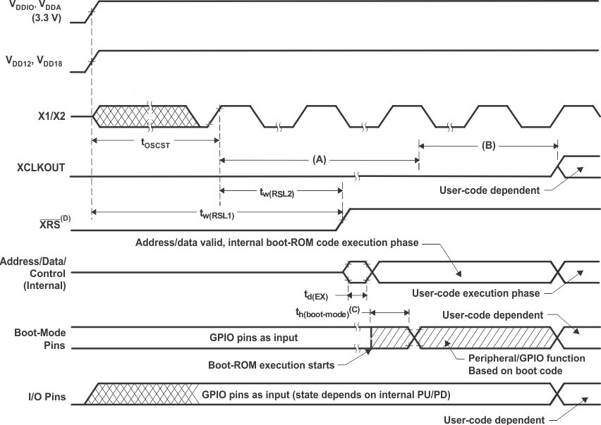
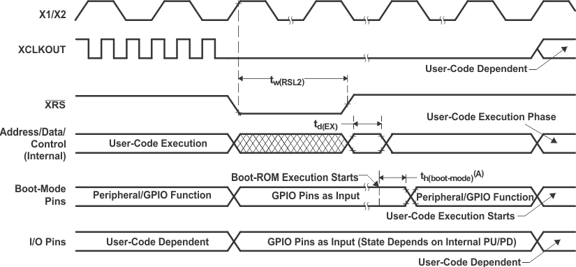
Table 5-3 Reset (XRS) Timing Requirements
| MIN | MAX | UNIT | ||
|---|---|---|---|---|
| th(boot-mode) | Hold time for boot-mode pins | 14000tc(M3C) | cycles | |
| tw(RSL2) | Pulse duration, XRS low | 32tc(OCK) | cycles | |
Table 5-4 Reset (XRS) Switching Characteristics
over recommended operating conditions (unless otherwise noted)| PARAMETER | MIN | TYP | MAX | UNIT | |
|---|---|---|---|---|---|
| tw(RSL1) | Pulse duration, XRS driven by device | 600 | μs | ||
| tw(WDRS) | Pulse duration, reset pulse generated by watchdog | 512tc(OCK) | cycles | ||
| td(EX) | Delay time, address/data valid after XRS high | 32tc(OCK) | cycles | ||
| tINTOSCST | Start-up time, internal zero-pin oscillator | 3 | μs | ||
| tOSCST (1) | On-chip crystal-oscillator start-up time | 2 | ms | ||
5.9.1.1 Power Management and Supervisory Circuit Solutions
LDO selection depends on the total power consumed in the end application. Go to www.ti.com and click on Power Management for a complete list of TI power ICs or select the Power Management Selection Guide link for specific power reference designs.
5.9.2 Clock Specifications
This section provides the frequencies and timing requirements of the input clocks; PLL lock times; frequencies of the internal clocks; and the frequency and switching characteristics of the output clock.
5.9.2.1 Changing the Frequency of the Main PLL
When configuring the PLL, it should be locked twice in a row. The PLL will be ready to use in the system when the xPLLSTS[xPLLLOCKS] bit is set after the second lock. The SysCtlClockPllConfig () function in sysctl.c, found in controlSUITE™, may be referenced as an example of a proper PLL initialization sequence. For additional information, see the "Clock Control" section of the Concerto F28M36x Technical Reference Manual (SPRUHE8).
5.9.2.2 Input Clock Frequency and Timing Requirements, PLL Lock Times
Table 5-5 shows the frequency requirements for the input clocks to the F28M36x devices. Table 5-6 shows the crystal equivalent series resistance requirements. Table 5-8, Table 5-9, Table 5-10, and Table 5-11 show the timing requirements for the input clocks to the F28M36x devices. Table 5-12 shows the PLL lock times for the Main PLL and the USB PLL. The Main PLL operates from the X1 or X1/X2 input clock pins, and the USB PLL operates from the XCLKIN input clock pin.
Table 5-5 Input Clock Frequency
| MIN | MAX | UNIT | |||
|---|---|---|---|---|---|
| f(OSC) | Frequency, X1/X2, from external crystal or resonator | 2 | 20 | MHz | |
| f(OCI) | Frequency, X1, from external oscillator (PLL enabled) | 2 | 30 | MHz | |
| f(OCI) | Frequency, X1, from external oscillator (PLL disabled) | 2 | 100 | MHz | |
| f(XCI) | Frequency, XCLKIN, from external oscillator | 2 | 60 | MHz | |
Table 5-6 Crystal Equivalent Series Resistance (ESR) Requirements(1)
| CRYSTAL FREQUENCY (MHz) | MAXIMUM ESR (Ω) (CL1/2 = 12 pF) |
MAXIMUM ESR (Ω) (CL1/2 = 24 pF) |
|---|---|---|
| 2 | 175 | 375 |
| 4 | 100 | 195 |
| 6 | 75 | 145 |
| 8 | 65 | 120 |
| 10 | 55 | 110 |
| 12 | 50 | 95 |
| 14 | 50 | 90 |
| 16 | 45 | 75 |
| 18 | 45 | 65 |
| 20 | 45 | 50 |
Table 5-7 Crystal Oscillator Electrical Characteristics
over recommended operating conditions (unless otherwise noted)| PARAMETER | TEST CONDITIONS | MIN | TYP | MAX | UNIT | |
|---|---|---|---|---|---|---|
| Start-up time(1) | f = 20 MHz; ESR MAX = 50 Ω; CL1 = CL2 = 24 pF, C0 = 7 pF |
2 | ms | |||
Table 5-8 X1 Timing Requirements - PLL Enabled(1)
| MIN | MAX | UNIT | |||
|---|---|---|---|---|---|
| tf(OCI) | Fall time, X1 | 6 | ns | ||
| tr(OCI) | Rise time, X1 | 6 | ns | ||
| tw(OCL) | Pulse duration, X1 low as a percentage of tc(OCI) | 45% | 55% | ||
| tw(OCH) | Pulse duration, X1 high as a percentage of tc(OCI) | 45% | 55% | ||
Table 5-9 X1 Timing Requirements - PLL Disabled
| MIN | MAX | UNIT | |||
|---|---|---|---|---|---|
| tf(OCI) | Fall time, X1 | Up to 20 MHz | 6 | ns | |
| 20 MHz to 100 MHz | 2 | ||||
| tr(OCI) | Rise time, X1 | Up to 20 MHz | 6 | ns | |
| 20 MHz to 100 MHz | 2 | ||||
| tw(OCL) | Pulse duration, X1 low as a percentage of tc(OCI) | 45% | 55% | ||
| tw(OCH) | Pulse duration, X1 high as a percentage of tc(OCI) | 45% | 55% | ||
Table 5-10 XCLKIN Timing Requirements - PLL Enabled(1)
| MIN | MAX | UNIT | |||
|---|---|---|---|---|---|
| tf(XCI) | Fall time, XCLKIN | 6 | ns | ||
| tr(XCI) | Rise time, XCLKIN | 6 | ns | ||
| tw(XCL) | Pulse duration, XCLKIN low as a percentage of tc(XCI) | 45% | 55% | ||
| tw(XCH) | Pulse duration, XCLKIN high as a percentage of tc(XCI) | 45% | 55% | ||
Table 5-11 XCLKIN Timing Requirements - PLL Disabled
| MIN | MAX | UNIT | |||
|---|---|---|---|---|---|
| tf(XCI) | Fall time, XCLKIN | Up to 20 MHz | 6 | ns | |
| 20 MHz to 100 MHz | 2 | ||||
| tr(XCI) | Rise time, XCLKIN | Up to 20 MHz | 6 | ns | |
| 20 MHz to 100 MHz | 2 | ||||
| tw(XCL) | Pulse duration, XCLKIN low as a percentage of tc(XCI) | 45% | 55% | ||
| tw(XCH) | Pulse duration, XCLKIN high as a percentage of tc(XCI) | 45% | 55% | ||
Table 5-12 PLL Lock Times
| MIN | NOM | MAX | UNIT | |||
|---|---|---|---|---|---|---|
| t(PLL) | Lock time, Main PLL (X1, from external oscillator) | 2000(1) | input clock cycles |
|||
| t(USB) | Lock time, USB PLL (XCLKIN, from external oscillator) | 2000(1) | input clock cycles |
|||
5.9.2.3 Output Clock Frequency and Switching Characteristics
Table 5-13 provides the frequency of the output clock from the F28M36x devices. Table 5-14 shows the switching characteristics of the output clock from the F28M36x devices, XCLKOUT.
Table 5-13 Output Clock Frequency
| MIN | MAX | UNIT | |||
|---|---|---|---|---|---|
| f(XCO) | Frequency, XCLKOUT | 2 | 37.5 | MHz | |
Table 5-14 XCLKOUT Switching Characteristics (PLL Bypassed or Enabled)(1)(2)
over recommended operating conditions (unless otherwise noted)| PARAMETER | MIN | MAX | UNIT | ||
|---|---|---|---|---|---|
| tf(XCO) | Fall time, XCLKOUT | 5 | ns | ||
| tr(XCO) | Rise time, XCLKOUT | 5 | ns | ||
| tw(XCOL) | Pulse duration, XCLKOUT low | H – 2 | H + 2 | ns | |
| tw(XCOH) | Pulse duration, XCLKOUT high | H – 2 | H + 2 | ns | |
5.9.2.4 Internal Clock Frequencies
Table 5-15 provides the clock frequencies for the internal clocks of the F28M36x devices.
Table 5-15 Internal Clock Frequencies (150-MHz Devices)
| MIN | NOM | MAX | UNIT | |||
|---|---|---|---|---|---|---|
| f(USB) | Frequency, USBPLLCLK | 60 | MHz | |||
| f(PLL) | Frequency, PLLSYSCLK | 2 | 150 | MHz | ||
| f(OCK) | Frequency, OSCCLK | 2 | 100 | MHz | ||
| f(M3C) | Frequency, M3SSCLK | 2 | 100(1) | MHz | ||
| f(ADC) | Frequency, ASYSCLK | 2 | 37.5 | MHz | ||
| f(SYS) | Frequency, C28SYSCLK | 2 | 150(1) | MHz | ||
| f(HSP) | Frequency, C28HSPCLK | 2 | 150(1) | MHz | ||
| f(LSP) | Frequency, C28LSPCLK(2) | 2 | 37.5(3) | 150(1) | MHz | |
| f(10M) | Frequency, 10MHZCLK | 10 | MHz | |||
| f(32K) | Frequency, 32KHZCLK | 32 | kHz | |||
5.9.3 Timing Parameter Symbology
Timing parameter symbols used are created in accordance with JEDEC Standard 100. To shorten the symbols, some of the pin names and other related terminology have been abbreviated as follows:
| Lowercase subscripts and their meanings: |
Letters and symbols and their meanings: |
||
|---|---|---|---|
| a | access time | H | High |
| c | cycle time (period) | L | Low |
| d | delay time | V | Valid |
| f | fall time | X | Unknown, changing, or don't care level |
| h | hold time | Z | High impedance |
| r | rise time | ||
| su | setup time | ||
| t | transition time | ||
| v | valid time | ||
| w | pulse duration (width) | ||
5.9.3.1 General Notes on Timing Parameters
All output signals from the 28x devices (including XCLKOUT) are derived from an internal clock such that all output transitions for a given half-cycle occur with a minimum of skewing relative to each other.
The signal combinations shown in the following timing diagrams may not necessarily represent actual cycles. For actual cycle examples, see the appropriate cycle description section of this document.
5.9.3.2 Test Load Circuit
This test load circuit is used to measure all switching characteristics provided in this document.

5.9.4 Flash Timing – Master Subsystem
Table 5-16 Master Subsystem – Flash/OTP Endurance
| MIN | TYP | MAX | UNIT | ||
|---|---|---|---|---|---|
| Nf | Flash endurance for the array (write/erase cycles) | 20000 | 50000 | cycles | |
| NOTP | OTP endurance for the array (write cycles) | 1 | write | ||
Table 5-17 Master Subsystem – Flash Parameters(2)
| PARAMETER | TEST CONDITIONS | MIN | TYP | MAX | UNIT | ||
|---|---|---|---|---|---|---|---|
| Program Time(1) | 128 data bits + 16 ECC bits | 40 | 300 | μs | |||
| 32K Sector | 290 | 580 | ms | ||||
| 128K Sector | 1160 | 2320 | ms | ||||
| Erase Time(3)
at < 25 cycles |
32K Sector | 25 | 50 | ms | |||
| 128K Sector | 40 | 70 | |||||
| Erase Time(3)
at 50k cycles |
32K Sector | 115 | 4000 | ms | |||
| 128K Sector | 140 | 4000 | |||||
| IDDP(4)(5) | VDD current consumption during Erase/Program cycle | VREG disabled | 105 | mA | |||
| IDDIOP(4)(5) | VDDIO current consumption during Erase/Program cycle | 55 | |||||
| IDDIOP(4)(5) | VDDIO current consumption during Erase/Program cycle | VREG enabled | 195 | mA | |||
- Code that uses Flash API to program the Flash
- Flash API itself
- Flash data to be programmed
Program time calculation is based on programming 144 bits at a time at the specified operating frequency. Program time includes Program verify by the CPU. Note that the program time does not degrade with write/erase (W/E) cycling, but the erase time does.
Erase time includes Erase verify by the CPU and does not involve any data transfer.
Table 5-18 Master Subsystem – Flash/OTP Access Timing(1)
| PARAMETER | MIN | MAX | UNIT | |
|---|---|---|---|---|
| ta(f) | Flash access time | 25 | ns | |
| ta(OTP) | OTP access time | 50 | ns | |
Table 5-19 Master Subsystem – Flash Data Retention Duration
| PARAMETER | TEST CONDITIONS | MIN | MAX | UNIT | |
|---|---|---|---|---|---|
| tretention | Data retention duration | TJ = 85°C | 20 | years | |
Table 5-20 Master Subsystem – Minimum Required Flash/OTP Wait States at Different Frequencies
| SYSCLKOUT (MHz) | SYSCLKOUT (ns) | WAIT STATE |
|---|---|---|
| 125 | 8 | 3 |
| 120 | 8.33 | 2 |
| 110 | 9.1 | 2 |
| 100 | 10 | 2 |
| 90 | 11.11 | 2 |
| 80 | 12.5 | 1 |
| 70 | 14.29 | 1 |
| 60 | 16.67 | 1 |
| 50 | 20 | 1 |
| 40 | 25 | 0 |
| 30 | 33.33 | 0 |
| 20 | 50 | 0 |
| 10 | 100 | 0 |
The equation to compute the Flash wait state in Table 5-20 is as follows:

round up to the next integer, or 1, whichever is larger.
5.9.5 Flash Timing – Control Subsystem
Table 5-21 Control Subsystem – Flash/OTP Endurance
| MIN | TYP | MAX | UNIT | ||
|---|---|---|---|---|---|
| Nf | Flash endurance for the array (write/erase cycles) | 20000 | 50000 | cycles | |
| NOTP | OTP endurance for the array (write cycles) | 1 | write | ||
Table 5-22 Control Subsystem – Flash Parameters(2)(6)
| PARAMETER | TEST CONDITIONS | MIN | TYP | MAX | UNIT | ||
|---|---|---|---|---|---|---|---|
| Program Time(1) | 128 data bits + 16 ECC bits | 40 | 300 | μs | |||
| 16K Sector | 105 | 210 | ms | ||||
| 64K Sector | 420 | 840 | ms | ||||
| Erase Time(3)
at < 25 cycles |
16K Sector | 25 | 50 | ms | |||
| 64K Sector | 30 | 55 | |||||
| Erase Time(3)
at 50k cycles |
16K Sector | 105 | 4000 | ms | |||
| 64K Sector | 115 | 4000 | |||||
| IDDP(4)(5) | VDD current consumption during Erase/Program cycle | VREG disabled | 90 | mA | |||
| IDDIOP(4)(5) | VDDIO current consumption during Erase/Program cycle | 55 | |||||
| IDDIOP(4)(5) | VDDIO current consumption during Erase/Program cycle | VREG enabled | 150 | mA | |||
- Code that uses Flash API to program the Flash
- Flash API itself
- Flash data to be programmed
Program time calculation is based on programming 144 bits at a time at the specified operating frequency. Program time includes Program verify by the CPU. Note that the program time does not degrade with write/erase (W/E) cycling, but the erase time does.
Erase time includes Erase verify by the CPU and does not involve any data transfer.
Table 5-23 Control Subsystem – Flash/OTP Access Timing(1)
| PARAMETER | MIN | MAX | UNIT | |
|---|---|---|---|---|
| ta(f) | Flash access time | 25 | ns | |
| ta(OTP) | OTP access time | 50 | ns | |
Table 5-24 Control Subsystem – Flash Data Retention Duration
| PARAMETER | TEST CONDITIONS | MIN | MAX | UNIT | |
|---|---|---|---|---|---|
| tretention | Data retention duration | TJ = 85°C | 20 | years | |
Table 5-25 Control Subsystem – Minimum Required Flash/OTP Wait States at Different Frequencies
| SYSCLKOUT (MHz) | SYSCLKOUT (ns) | WAIT STATE |
|---|---|---|
| 150 | 6.7 | 3 |
| 140 | 7.14 | 3 |
| 130 | 7.7 | 3 |
| 120 | 8.33 | 2 |
| 110 | 9.1 | 2 |
| 100 | 10 | 2 |
| 90 | 11.11 | 2 |
| 80 | 12.5 | 1 |
| 70 | 14.29 | 1 |
| 60 | 16.67 | 1 |
| 50 | 20 | 1 |
| 40 | 25 | 0 |
| 30 | 33.33 | 0 |
| 20 | 50 | 0 |
| 10 | 100 | 0 |
The equation to compute the Flash wait state in Table 5-25 is as follows:

round up to the next integer, or 1, whichever is larger.
5.9.6 GPIO Electrical Data and Timing
5.9.6.1 GPIO - Output Timing
Table 5-26 General-Purpose Output Switching Characteristics
over recommended operating conditions (unless otherwise noted)| PARAMETER | MIN | MAX | UNIT | ||
|---|---|---|---|---|---|
| tr(GPO) | Rise time, GPIO switching low to high | All GPIOs | 8 | ns | |
| tf(GPO) | Fall time, GPIO switching high to low | All GPIOs | 8 | ns | |
| tfGPO | Toggling frequency, GPIO pins | 25 | MHz | ||
 Figure 5-4 General-Purpose Output Timing
5.9.6.2 GPIO - Input Timing
Table 5-27 General-Purpose Input Timing Requirements
| MIN | MAX | UNIT | |||
|---|---|---|---|---|---|
| tw(SP) | Sampling period | QUALPRD = 0 | 1tc(SCO) | cycles | |
| QUALPRD ≠ 0 | 2tc(SCO) * QUALPRD | cycles | |||
| tw(IQSW) | Input qualifier sampling window | tw(SP) * (n(1) – 1) | cycles | ||
| tw(GPI) (2) | Pulse duration, GPIO low/high | Synchronous mode | 2tc(SCO) | cycles | |
| With input qualifier | tw(IQSW) + tw(SP) + 1tc(SCO) | cycles | |||
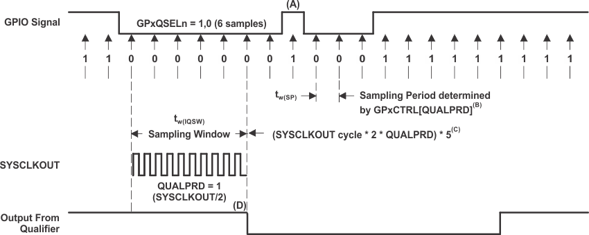
5.9.6.3 Sampling Window Width for Input Signals
The following section summarizes the sampling window width for input signals for various input qualifier configurations.
Sampling frequency denotes how often a signal is sampled with respect to SYSCLKOUT.
Sampling frequency = SYSCLKOUT/(2 * QUALPRD), if QUALPRD ≠ 0
Sampling frequency = SYSCLKOUT, if QUALPRD = 0
Sampling period = SYSCLKOUT cycle × 2 × QUALPRD, if QUALPRD ≠ 0
In the above equations, SYSCLKOUT cycle indicates the time period of SYSCLKOUT.
Sampling period = SYSCLKOUT cycle, if QUALPRD = 0
In a given sampling window, either 3 or 6 samples of the input signal are taken to determine the validity of the signal. This is determined by the value written to GPxQSELn register.
Case 1:
Qualification using 3 samples
Sampling window width = (SYSCLKOUT cycle × 2 × QUALPRD) × 2, if QUALPRD ≠ 0
Sampling window width = (SYSCLKOUT cycle) × 2, if QUALPRD = 0
Case 2:
Qualification using 6 samples
Sampling window width = (SYSCLKOUT cycle × 2 × QUALPRD) × 5, if QUALPRD ≠ 0
Sampling window width = (SYSCLKOUT cycle) × 5, if QUALPRD = 0
 Figure 5-6 General-Purpose Input Timing
5.9.6.4 Low-Power Mode Wakeup Timing
Table 5-28 shows the timing requirements, Table 5-29 shows the switching characteristics, and Figure 5-7 shows the timing diagram for IDLE mode.
Table 5-28 IDLE Mode Timing Requirements(1)
| MIN | MAX | UNIT | |||
|---|---|---|---|---|---|
| tw(WAKE-INT) | Pulse duration, external wake-up signal | Without input qualifier | 2tc(SCO) | cycles | |
| With input qualifier | 5tc(SCO) + tw(IQSW) | ||||
Table 5-29 IDLE Mode Switching Characteristics(1)
over recommended operating conditions (unless otherwise noted)| PARAMETER | TEST CONDITIONS | MIN | MAX | UNIT | |
|---|---|---|---|---|---|
| td(WAKE-IDLE) | Delay time, external wake signal to program execution resume (2) | ||||
Wake-up from Flash
|
Without input qualifier | 20tc(SCO) | cycles | ||
| With input qualifier | 20tc(SCO) + tw(IQSW) | ||||
Wake-up from Flash
|
Without input qualifier | 1050tc(SCO) | cycles | ||
| With input qualifier | 1050tc(SCO) + tw(IQSW) | ||||
|
Without input qualifier | 20tc(SCO) | cycles | ||
| With input qualifier | 20tc(SCO) + tw(IQSW) | ||||

Table 5-30 STANDBY Mode Timing Requirements
| MIN | MAX | UNIT | ||||
|---|---|---|---|---|---|---|
| tw(WAKE-INT) | Pulse duration, external wake-up signal | Without input qualification | 3tc(OSCCLK) | cycles | ||
| With input qualification(1) | (2 + QUALSTDBY) * tc(OSCCLK) | |||||
Table 5-31 STANDBY Mode Switching Characteristics
over recommended operating conditions (unless otherwise noted)| PARAMETER | TEST CONDITIONS | MIN | MAX | UNIT | |
|---|---|---|---|---|---|
| td(IDLE-XCOL) | Delay time, IDLE instruction executed to XCLKOUT low | 32tc(SCO) | 45tc(SCO) | cycles | |
| td(WAKE-STBY) | Delay time, external wake signal to program execution resume(1) | cycles | |||
|
Without input qualifier | 100tc(SCO) | cycles | ||
| With input qualifier | 100tc(SCO) + tw(WAKE-INT) | ||||
|
Without input qualifier | 1125tc(SCO) | cycles | ||
| With input qualifier | 1125tc(SCO) + tw(WAKE-INT) | ||||
|
Without input qualifier | 100tc(SCO) | cycles | ||
| With input qualifier | 100tc(SCO) + tw(WAKE-INT) | ||||
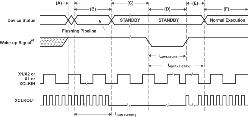
- 16 cycles, when DIVSEL = 00 or 01
- 32 cycles, when DIVSEL = 10
- 64 cycles, when DIVSEL = 11
This delay enables the CPU pipeline and any other pending operations to flush properly. If an access to XINTF is in progress and its access time is longer than this number then it will fail. It is recommended to enter STANDBY mode from SARAM without an XINTF access in progress.
Table 5-32 HALT Mode Timing Requirements
| MIN | MAX | UNIT | |||
|---|---|---|---|---|---|
| tw(WAKE-GPIO) | Pulse duration, GPIO wake-up signal | toscst + 2tc(OSCCLK)(1) | cycles | ||
| tw(WAKE-XRS) | Pulse duration, XRS wakeup signal | toscst + 8tc(OSCCLK) | cycles | ||
Table 5-33 HALT Mode Switching Characteristics
over recommended operating conditions (unless otherwise noted)| PARAMETER | MIN | MAX | UNIT | |
|---|---|---|---|---|
| td(IDLE-XCOL) | Delay time, IDLE instruction executed to XCLKOUT low | 32tc(SCO) | 45tc(SCO) | cycles |
| tp | PLL lock-up time | 131072tc(OSCCLK) | cycles | |
| td(WAKE-HALT) | Delay time, PLL lock to program execution resume
|
1125tc(SCO) | cycles | |
|
35tc(SCO) | cycles | ||
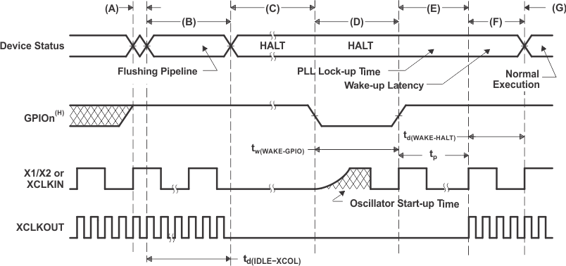
- 16 cycles, when DIVSEL = 00 or 01
- 32 cycles, when DIVSEL = 10
- 64 cycles, when DIVSEL = 11
5.9.7 External Interrupt Electrical Data and Timing
Table 5-34 External Interrupt Timing Requirements(1)
| MIN | MAX | UNIT | |||
|---|---|---|---|---|---|
| tw(INT) (2) | Pulse duration, INT input low/high | Synchronous | 1tc(SCO) | cycles | |
| With qualifier | 1tc(SCO) + tw(IQSW) | cycles | |||
Table 5-35 External Interrupt Switching Characteristics(1)
over recommended operating conditions (unless otherwise noted)| PARAMETER | MIN | MAX | UNIT | |
|---|---|---|---|---|
| td(INT) | Delay time, INT low/high to interrupt-vector fetch | tw(IQSW) + 12tc(SCO) | cycles | |
 Figure 5-10 External Interrupt Timing
5.10 Analog and Shared Peripherals
Concerto Shared Peripherals are accessible from both the Master Subsystem and the Control Subsystem. The Analog Shared Peripherals include two 12-bit ADCs (Analog-to-Digital Converters), and six Comparator + DAC (10-bit) modules. The ADC Result Registers are accessible by CPUs and DMAs of the Master and Control Subsystems. All other analog registers, such as the ADC Configuration and Comparator Registers, are accessible by the C28x CPU only. The Digital Shared Peripherals include the IPC peripheral and the EPI. IPC is accessible by both CPUs; EPI is accessible by both CPUs and both DMAs.
IPC is used for sending and receiving synchronization events between Master and Control subsystems to coordinate execution of software running on both processors, or exchanging of data between the two processors. EPI is used by this device to communicate with external memory and other devices.
For detailed information on the processor peripherals, see the Concerto F28M36x Technical Reference Manual (SPRUHE8).
5.10.1 Analog-to-Digital Converter
Figure 5-11 shows the internal structure of each of the two ADC peripherals that are present on Concerto. Each ADC has 16 channels that can be programmed to select analog inputs, select start-of-conversion trigger, set the sampling window, and select end-of-conversion interrupt to prompt a CPU or DMA to read 16 result registers. The 16 ADC channels can be used independently or in pairs, based on the assignments inside the SAMPLEMODE register. Pairing up the channels allows two analog inputs to be sampled simultaneously—thereby, increasing the overall conversion performance.
5.10.1.1 Sample Mode
Each ADC has 16 programmable channels that can be independently programmed for analog-to-digital conversion when corresponding bits in the SAMPLEMODE register are set to Sequential Mode. For example, if bit 2 in the SAMPLEMODE register is set to 0, ADC channels 4 and 5 are set to sequential mode. Both the SOC4CTL and SOC5CTL registers can then be programmed to configure channels 4 and 5 to independently perform analog-to-digital conversions with results being stored in the RESULT4 and RESULT5 registers. "Independently" means that channel 4 may use a different SOC trigger, different analog input, and different sampling window than the trigger, input, and window assigned to channel 5.
The 16 programmable channels for each ADC may also be grouped in 8 channel pairs when corresponding bits in the SAMPLEMODE register are set to Simultaneous Mode. For example, if bit 2 in the SAMPLEMODE register is set to 1, ADC channels 4 and 5 are set to Simultaneous Mode. The SOC4CTL register now contains configuration parameters for both channel 4 and channel 5, and the SOC5CTL register is ignored. While channel 4 and channel 5 are still using dedicated analog inputs (now selected as pairs in the CHSEL field of SOC4CTL), they both share the same SOC trigger and Sampling Window, with the results being stored in the RESULT4 and RESULT5 registers.
The Simultaneous mode is made possible by two sample-and-hold units present in each ADC. Each sample-and-hold unit has its own mux for selecting analog inputs (see Figure 5-11). By programming the SAMPLEMODE register, the 16 available channels can be configured as 16 independent channels, 8 channel pairs, or any combination thereof (for example, 10 sequential channels and 3 simultaneous pairs).
 Figure 5-11 ADC
5.10.1.2 Start-of-Conversion Triggers
There are eight external SOC triggers that go to each of the two ADC modules (from the Control Subsystem). In addition to the eight external SOC triggers, there are also two internal SOC triggers derived from EOC interrupts inside each ADC module (ADCINT1 and ADCINT2). Registers INTSOCSEL1 and 2 are used to configure each of the 16 ADC channels for internal or external SOC sources. If internal SOC is chosen for a given channel, the INTSOCSEL1 and 2 registers also select whether the internal source is ADCINT1 or ADCINT2. If external SOC is chosen for a given ADC channel, the TRIGSEL field of the corresponding SOCxCTL register selects which of the eight external triggers is used for SOC in that channel. One analog-to-digital conversion can be performed at a time by the 12-bit ADC. The analog-to-digital conversion priority is managed according to the state of the PRICTL register.
5.10.1.3 Analog Inputs
Analog inputs to each of the two ADC modules are organized in two groups—A and B, with each group having a dedicated mux and sample-and-hold unit (see Figure 5-11). Mux A selects one of six possible analog inputs via AIO MUX. Mux B selects one of seven possible analog inputs—six external inputs via AIO MUX, and one from the internal VREFLO signal, which is currently tied to the Analog Ground. The Mux A and Mux B inputs can be simultaneously or sequentially sampled by the two sample-and-hold units according to the sampling window chosen in the SOCxCTL register for the corresponding channel.
5.10.1.4 ADC Result Registers and EOC Interrupts
Concerto analog-to-digital conversion results are stored in 32 Results Registers (16 for ADC1 and 16 for ADC2). The 16 ADCx channels can be programmed via the INTSELxNy registers to trigger up to eight ADCINT interrupts per ADC module, when their results are ready to be read. The eight ADCINT interrupts from ADC1 and the eight ADCINT interrupts from ADC2 are AND-ed together before propagating to both the Master Subsystem and the Control Subsystem, announcing that the Result Registers are ready to be read by a CPU or DMA (see Figure 6-3).
5.10.1.5 ADC Electrical Data and Timing
Table 5-36 ADC Electrical Characteristics
over recommended operating conditions (unless otherwise noted)| PARAMETER | MIN | TYP | MAX | UNIT | |
|---|---|---|---|---|---|
| DC SPECIFICATIONS | |||||
| Resolution | 12 | Bits | |||
| ADC clock | 2 | 37.5 | MHz | ||
| Sample Window | 7 | 64 | ADC clocks | ||
| ACCURACY | |||||
| INL (Integral nonlinearity) | –4 | 4 | LSB | ||
| DNL (Differential nonlinearity) | –1 | 1.5 | LSB | ||
| Offset error | Executing a single self-recalibration | –20 | 0 | 20 | LSB |
| Executing periodic self-recalibration | –4 | 0 | 4 | ||
| Overall gain error with internal reference | –60 | 60 | LSB | ||
| Overall gain error with external reference | –40 | 40 | LSB | ||
| Channel-to-channel offset variation | –4 | 4 | LSB | ||
| Channel-to-channel gain variation | –4 | 4 | LSB | ||
| VREFLO input current | –100 | µA | |||
| VREFHI input current | 100 | µA | |||
| ANALOG INPUT | |||||
| Analog input voltage with internal reference | 0 | 3.3 | V | ||
| Analog input voltage with external reference | VREFLO | VREFHI | V | ||
| VREFLO input voltage | VSSA | 0.66 | V | ||
| VREFHI input voltage | 2.64 | VDDA | V | ||
| Input capacitance | 5 | pF | |||
| Input leakage current | ±2 | μA | |||
| ADDITIONAL | |||||
| ADC SNR | 65 | dB | |||
| ADC SINAD | 62 | dB | |||
| ADC THD (50 kHz) | –65 | dB | |||
| ENOB (SNR) | 10.1 | Bits | |||
| SFDR | 66 | dB | |||
![F28M36P63C2 F28M36P53C2 F28M36H53C2 F28M36H53B2 F28M36H33C2 F28M36H33B2 Typical ADC Total
Error
[Temperature (°C) versus Total Error (LSBs)] F28M36P63C2 F28M36P53C2 F28M36H53C2 F28M36H53B2 F28M36H33C2 F28M36H33B2 adc_graph_prs825.gif](/ods/images/ZHCSBK0D/adc_graph_prs825.gif)
[Temperature (°C) versus Total Error (LSBs)]
Table 5-37 External ADC Start-of-Conversion Switching Characteristics
over recommended operating conditions (unless otherwise noted)| PARAMETER | MIN | MAX | UNIT | |
|---|---|---|---|---|
| tw(ADCSOCL) | Pulse duration, ADCSOCxO low | 32tc(HCO) | cycles | |
 Figure 5-13 ADCSOCAO or ADCSOCBO Timing
5.10.2 Comparator + DAC Units
Figure 5-14 shows the internal structure of the six analog Comparator + DAC units present in Concerto devices. Each unit compares two analog inputs (A and B) and assigns a value of ‘1’ when the voltage of the A input is greater than that of the B input, or a value of ‘0’ when the opposite is true. The six A inputs and six B inputs come from AIO_MUX1 and AIO_MUX2. All six B inputs can also be provided by the 10-bit digital-to-analog units that are present in each comparator DAC. The 10-bit value for each DAC unit is programmed in the respective DACVAL register. Another comparator register, COMPCTL, can be programmed to select the source of the B input, to enable or disable the comparator circuit, to invert comparator output, to synchronize comparator output to C28x SYSCLK, and to select the qualification period (number of clock cycles). All six output signals from the six comparators can be routed out to the device pins via GPIO_MUX2 pin mux.
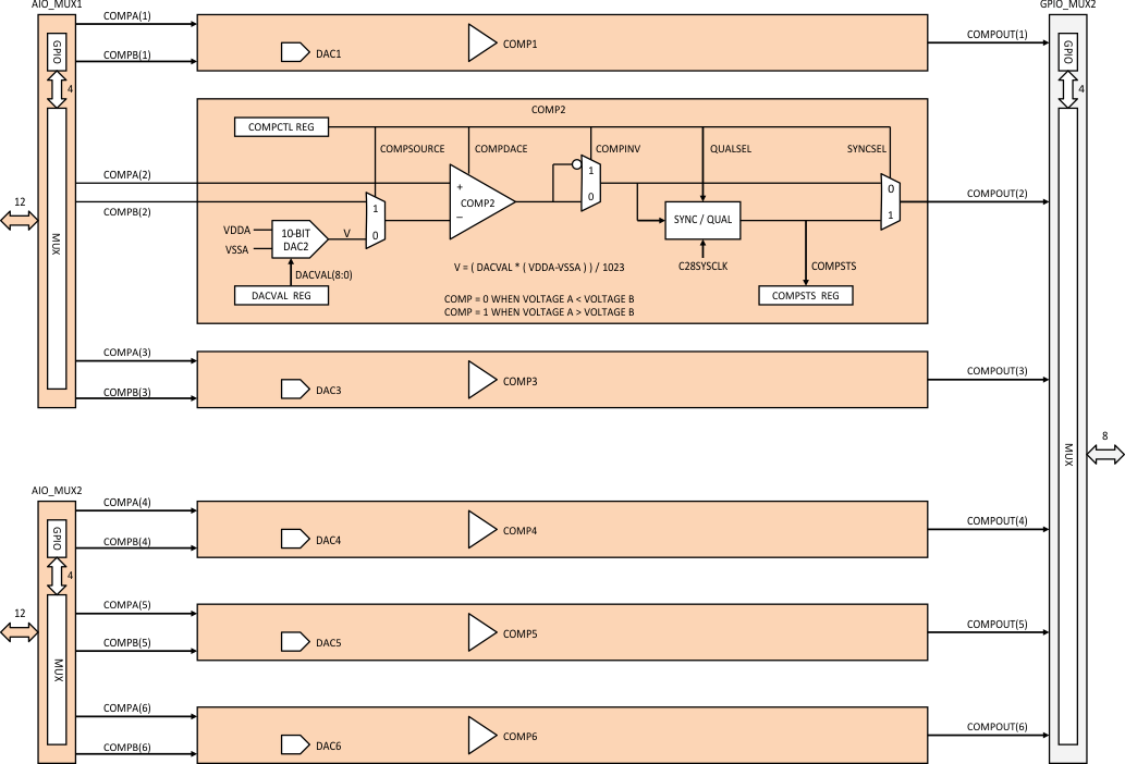 Figure 5-14 Comparator + DAC Units
5.10.2.1 On-Chip Comparator and DAC Electrical Data and Timing
Table 5-38 Electrical Characteristics of the Comparator/DAC
over recommended operating conditions (unless otherwise noted)| PARAMETER | MIN | TYP | MAX | UNITS |
|---|---|---|---|---|
| Comparator | ||||
| Comparator Input Range | VSSA – VDDA | V | ||
| Comparator response time to PWM Trip Zone (Async) | 30 | ns | ||
| Input Offset | ±5 | mV | ||
| Input Hysteresis(1) | 35 | mV | ||
| DAC | ||||
| DAC Output Range | VSSA – VDDA | V | ||
| DAC resolution | 10 | bits | ||
| DAC settling time | See Figure 5-15 | |||
| DAC Gain | –1.5 | % | ||
| DAC Offset | 10 | mV | ||
| Monotonic | Yes | |||
| INL | ±3 | LSB | ||
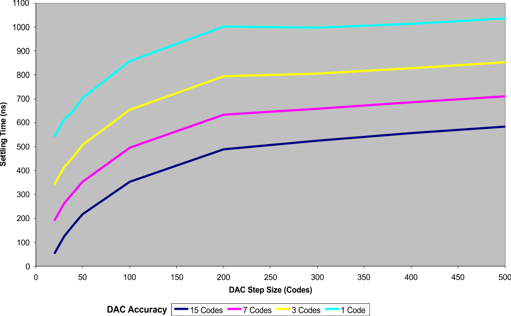 Figure 5-15 DAC Settling Time
5.10.3 Interprocessor Communications
Figure 5-16 shows the internal structure of the IPC peripheral used to synchronize program execution and exchange of data between the Cortex-M3 and the C28x CPU. IPC can be used by itself when synchronizing program execution or it can be used in conjunction with Message RAMs when coordinating data transfers between processors. In either case, the operation of the IPC is the same. There are two independent sides to the IPC peripheral—MTOC (Master to Control) and CTOM (Control to Master).
The MTOC IPC is used by the Master Subsystem to send events to the Control Subsystem. The MTOC IPC typically sends events to the Control Subsystem by using the following registers: MTOCIPCSET, MTOCIPCFLG/MTOCIPCSTS (1), and MTOCIPCACK. Each of the 32 bits of these registers represents 32 independent channels through which the Cortex-M3 CPU can send up to 32 events to the C28x CPU via software handshaking. Additionally, the first 4 bits of the MTOCIPC registers are supplemented with interrupts. To send an event via channel 2 from Cortex-M3 to C28x, for example, the Cortex-M3 and C28x CPUs use bit 2 of the MTOCIPCSET, MTOCIPCFLG/MTOCIPCSTS, MTOCIPCACK registers. The handshake starts with the Cortex-M3 polling bit 2 of the MTOCIPCFLG register to make sure bit 2 is ‘0’. Next, the Cortex-M3 writes a ‘1’ into bit 2 of the MTOCIPCSET register to start the handshake. In the mean time, the C28x is continually polling the MTOCIPCSTS register while waiting for the message. As soon as the Cortex-M3 writes ‘1’ to bit 2 of the MTOCIPCSET register, bit 2 of MTOCIPCFLG/MTOCIPCSTS also turns ‘1’, thus announcing the event to the C28x. As soon as the C28x CPU reads a ‘1’ from the MTOCIPCSTS register, the C28x CPU should acknowledge by writing a ‘1’ to bit 2 of the MTOCIPCACK register, which in turn, clears bit 2 of the MTOCIPCFLG/MTOCIPCSTS register, enabling the Cortex-M3 to send another message. Because the first four channels (bits 0, 1, 2, 3) are backed up by interrupts, both processors in the above example can use IPC interrupt 2 instead of polling to increase performance.
A similar handshake is also used when sending data (not just event) from the Master Subsystem to the Control Subsystem, but with two additional steps. Before setting a bit in the MTOCIPCSET register, the Cortex-M3 should first load the MTOC Message RAM with a block of data that is to be made available to the C28x. In the second additional step, the C28x should read the data before setting a bit in the MTOCIPCACK register. This way, no data gets lost during multiple data transfers through a given block of the message RAM.
The CTOM IPC is used by the Control Subsystem to send events to the Master Subsystem. The CTOM IPC typically sends events to the Master Subsystem by using the following three registers: CTOMIPCSET, CTOMIPCFLG/CTOMIPCSTS, and CTOMIPCACK. The process is exactly the same as that for the MTOC IPC communication above.
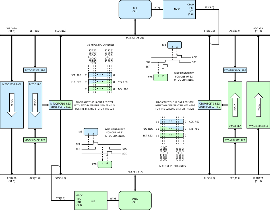 Figure 5-16 IPC
5.10.4 External Peripheral Interface
The EPI provides a high-speed parallel bus for interfacing external peripherals and memory. EPI is accessible from both the Master Subsystem and the Control Subsystem. EPI has several modes of operation to enable glueless connectivity to most types of external devices. Some EPI modes of operation conform to standard microprocessor address/data bus protocols, while others are tailored to support a variety of fast custom interfaces, such as those communicating with field-programmable gate arrays (FPGAs) and complex programmable logic devices (CPLDs).
The EPI peripheral can be accessed by the Cortex-M3 CPU, the Cortex-M3 DMA, the C28x CPU, and the C28x DMA over the high-performance AHB bus. The Cortex-M3 CPU and the µDMA drive AHB bus cycles directly through the Cortex-M3 Bus Matrix. The C28x CPU and DMA also connect to the Cortex-M3 Bus Matrix, but not directly. Before entering the Cortex-M3 Bus Matrix, the native C28x CPU and DMA bus cycles are first converted to AHB protocol inside the MEM32-to-AHB Bus Bridge. After that, they pass through the Frequency Gasket to reduce the bus frequency by a factor of 2 or 4. Inside the Cortex-M3 Bus Matrix, the Cortex-M3 bus cycles may have to compete with C28x bus cycles for access to the AHB bus on the way to the EPI peripheral. See Figure 5-17 to see how EPI interfaces to the Concerto Master Subsystem, the Concerto Control Subsystem, Resets, Clocks, and Interrupts.
NOTE
The Control Subsystem has no direct access to EPI in silicon revision 0 devices.
Depending on how the Real-Time Window registers are configured inside the Bus Matrix, the arbitration between the Cortex-M3 and C28x bus cycles is fixed-priority with Cortex-M3 having higher priority than C28x, or the C28x having the option to own the Bus Matrix for a fixed period of time (window)—effectively stalling all Cortex-M3 accesses during that time. Another EPI register inside the Cortex-M3 Bus Matrix is the Memory Protection Register, which enables assignments of chip-select spaces to Cortex-M3 or C28x EPI accesses (or both). The assignments of chip-select spaces prevent a bus cycle (from any processor) that does not own a given chip-select space, from getting through to EPI. The Real-time Window registers are the only EPI-related registers that are configurable by the C28x. The Memory Protection Register is configurable only by the Cortex-M3 CPU, as are all configuration registers inside the EPI peripheral. Figure 5-17 shows the EPI registers and how they relate to individual blocks within the EPI.
Once a bus cycle arrives at the AHB bus interface inside the EPI peripheral, the bus cycle is routed to the General-Purpose Block, SDRAM Block, or the Host Bus Module, depending on the operating mode chosen through the EPI Configuration Register. Write cycles are buffered in a 4-word-deep Write FIFO; therefore, in most cases, the write cycles do not stall the CPU or DMA unless the Write FIFO becomes full. Read cycles can be handled in two different ways: blocking read cycles and nonblocking read cycles. Blocking read cycles are implemented when the content of a Read Data Register is 0. Blocking reads stall the CPU or DMA until the bus transaction completes. Nonblocking read cycles are triggered when a non-zero value is written into a Read Data Register. A non-zero value being written into a Read Data register triggers EPI to autonomously perform multiple data reads in the background (without involving CPU or DMA) according to values stored inside the Read Address Register and the Read Size Register. The incoming data is then temporarily stored in the Non-Blocking Read (NBR) FIFO until an EPI interrupt is generated to prompt the CPU or DMA to read the FIFO without risk of stalling. Furthermore, EPI has actually two sets of Data/Address/Size registers (set 0 and set 1) to enable ping-pong operation of nonblocking reads. In a ping-pong operation, while the previously fetched data is being read by the CPU or DMA from one end of the NBR FIFO, the next set of data words is simultaneously being deposited into the other end of the NBR FIFO.
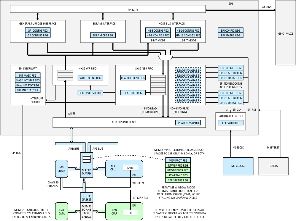 Figure 5-17 EPI
EPI can directly interrupt the Cortex-M3 CPU, the Cortex-M3 uDMA, and the C28x CPU (but not the C28x DMA) via the EPI interrupt. Typically, EPI interrupts are used to prompt the CPU or DMA to move data to and from EPI. There are four EPI Interrupt registers that control various facets of interrupt generation, clearing, and masking. The EPI Interrupt can trigger µDMA to perform reads and writes through DMA Channels 20 and 22. If a CPU is the intended recipient, the Cortex-M3 CPU is interrupted by NVIC vector 69, and the C28x CPU is interrupted through the INT12/INTx6 vector to the PIE.
During EPI bus cycles, addresses entering the EPI module can propagate unchanged to the pins, or be remapped to different addresses according to values stored in the EPI Address Map Register in conjunction with the most significant bit of the incoming address.
The EPI's three primary operating modes are: the General-Purpose Mode, the SDRAM Mode, and the Host Bus Mode (including 8-bit and 16-bit versions).
5.10.4.1 EPI General-Purpose Mode
The EPI General-Purpose Mode is designed for high-speed clocked interfaces such as ones communicating with FPGAs and CPLDs. The high-speed clocked interfaces are different from the slower Host Bus interfaces, which have more relaxed timings that are compatible with established protocols like ones used to communicate with 8051 devices. Support of bus cycle framing and precisely controlled clocking are the additional features of the General-Purpose Mode that differentiate the General-Purpose Mode from the 8-bit and 16-bit Host Bus Modes.
Framing allows multiple bus transactions to be grouped together with an output signal called FRAME. The slave device responding to the bus cycles may use this signal to recognize related words of data and to speed up their transfers. The frame lengths are programmable and may vary from 1 to 30 clocks, depending on the clocking mode used.
Precise clocking is accomplished with a dedicated clock output pin (CLK). Devices responding the bus cycles can synchronize to CLK for faster transfers. The clock frequency can be precisely controlled through the Baud Rate Control block. This output clock can be gated or free-running. A gated approach uses a setup-time model in which the EPI clock controls when bus transactions are starting and stopping. A free-running EPI clock requires another method for determining when data is live, such as the frame pin or RD/WR strobes.
These and numerous other aspects of the General-Purpose Mode are controlled through the General-Purpose Configuration Register and the General-Purpose Configuration2 Register. The clocking for the General-Purpose Mode is configured through the EPI Baud Register of the EPI Baud Rate Control block.
See Figure 5-18 for a snapshot of the General-Purpose Mode registers, modes, and features. For more detailed maps of the General-Purpose Mode, see Table 5-39.
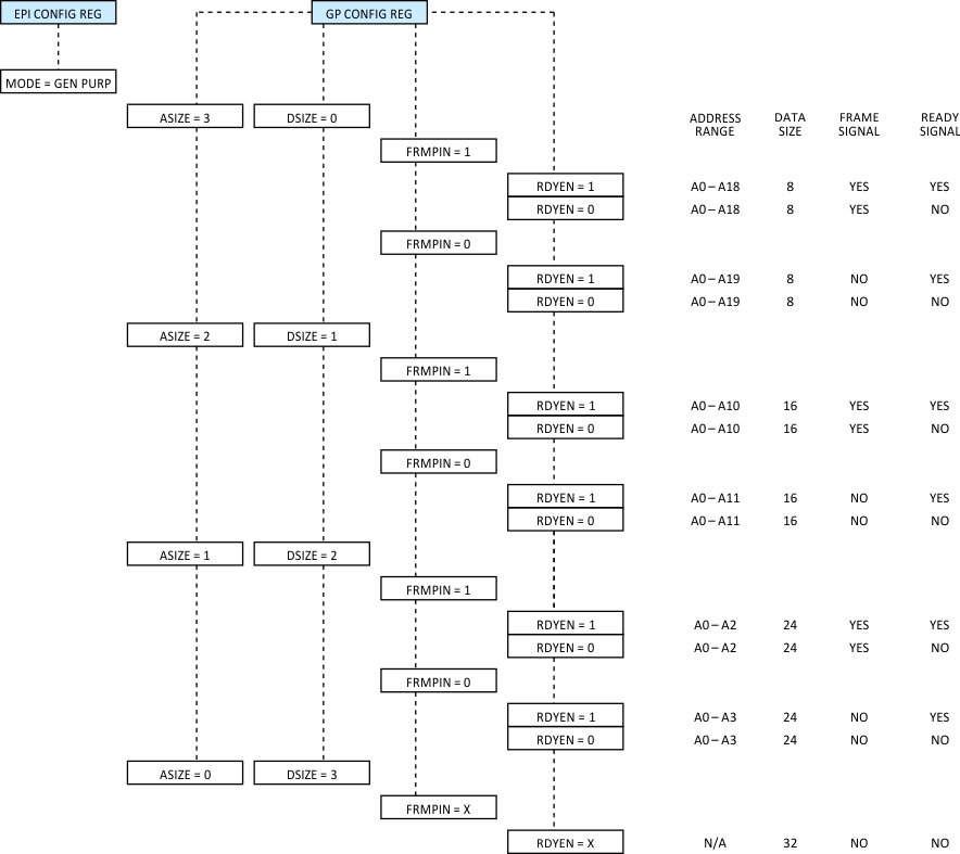 Figure 5-18 EPI General-Purpose Modes
Table 5-39 EPI MODES – General-Purpose Mode (EPICFG/MODE = 0x0)
| EPI PORT NAME | EPI SIGNAL FUNCTION | DEVICE PIN | |||||
|---|---|---|---|---|---|---|---|
| ACCESSIBLE BY Cortex-M3 | ACCESSIBLE BY C28x | GENERAL-PURPOSE SIGNAL (D8, A20) |
GENERAL-PURPOSE SIGNAL (D16, A12) |
GENERAL-PURPOSE SIGNAL (D24, A4) |
GENERAL-PURPOSE SIGNAL (D30, NO ADDR) |
(AVAILABLE GPIOMUX_1 MUXING CHOICES FOR EPI) |
|
| EPI0S0 | D0 | D0 | D0 | D0 | PH3_GPIO51 | ||
| EPI0S1 | D1 | D1 | D1 | D1 | PH2_GPIO50 | ||
| EPI0S2 | D2 | D2 | D2 | D2 | PC4_GPIO68 | ||
| EPI0S3 | D3 | D3 | D3 | D3 | PC5_GPIO69 | ||
| EPI0S4 | D4 | D4 | D4 | D4 | PC6_GPIO70 | ||
| EPI0S5 | D5 | D5 | D5 | D5 | PC7_GPIO71 | ||
| EPI0S6 | D6 | D6 | D6 | D6 | PH0_GPIO48 | ||
| EPI0S7 | D7 | D7 | D7 | D7 | PH1_GPIO49 | ||
| EPI0S8 | A0 | D8 | D8 | D8 | PE0_GPIO24 | ||
| EPI0S9 | A1 | D9 | D9 | D9 | PE1_GPIO25 | ||
| EPI0S10 | A2 | D10 | D10 | D10 | PH4_GPIO52 | ||
| EPI0S11 | A3 | D11 | D11 | D11 | PH5_GPIO53 | ||
| EPI0S12 | A4 | D12 | D12 | D12 | PF4_GPIO36 | ||
| EPI0S13 | A5 | D13 | D13 | D13 | PG0_GPIO40 | ||
| EPI0S14 | A6 | D14 | D14 | D14 | PG1_GPIO41 | ||
| EPI0S15 | A7 | D15 | D15 | D15 | PF5_GPIO37 | ||
| EPI0S16 | A8 | A0 | D16 | D16 | PJ0_GPIO56 | ||
| EPI0S17 | A9 | A1 | D17 | D17 | PJ1_GPIO57 | ||
| EPI0S18 | A10 | A2 | D18 | D18 | PJ2_GPIO58 | ||
| EPI0S19 | A11 | A3 | D19 | D19 | PD4_GPIO20 | PJ3_GPIO59 | |
| EPI0S20 | A12 | A4 | D29 | D29 | PD2_GPIO18 | ||
| EPI0S21 | A13 | A5 | D21 | D21 | PD3_GPIO19 | ||
| EPI0S22 | A14 | A6 | D22 | D22 | PB5_GPIO13 | ||
| EPI0S23 | A15 | A7 | D23 | D23 | PB4_GPIO12 | ||
| EPI0S24 | A16 | A8 | A0 | D24 | PE2_GPIO26 | ||
| EPI0S25 | A17 | A9 | A1 | D25 | PE3_GPIO27 | ||
| EPI0S26 | A18 | A10 | A2 | D26 | PH6_GPIO54 | ||
| EPI0S27 | A19/RDY | A11/RDY | A3/RDY | D27 | PH7_GPIO55 | ||
| EPI0S28 | WR | WR | WR | D28 | PD5_GPIO21 | PJ4_GPIO60 | |
| EPI0S29 | RD | RD | RD | D29 | PD6_GPIO22 | PJ5_GPIO61 | |
| EPI0S30 | FRAME | FRAME | FRAME | D30 | PD7_GPIO23 | PJ6_GPIO62 | |
| EPI0S31 | CLK | CLK | CLK | D31 | PG7_GPIO47 | ||
| EPI0S32 | x | x | x | x | PF2_GPIO34 | PC0_GPIO64 | |
| EPI0S33 | x | x | x | x | PF3_GPIO35 | PC1_GPIO65 | |
| EPI0S34 | x | x | x | x | PE4_GPIO28 | ||
| EPI0S35 | x | x | x | x | PE5_GPIO29 | ||
| EPI0S36 | x | x | x | x | PB7_GPIO15 | PC3_GPIO67 | |
| EPI0S37 | x | x | x | x | PB6_GPIO14 | PC2_GPIO66 | |
| EPI0S38 | x | x | x | x | PF6_GPIO38 | PE4_GPIO28 | |
| EPI0S39 | x | x | x | x | PG2_GPIO42 | ||
| EPI0S40 | x | x | x | x | PG5_GPIO45 | ||
| EPI0S41 | x | x | x | x | PG6_GPIO46 | ||
| EPI0S42 | x | x | x | x | PN6_GPIO102 | ||
| EPI0S43 | x | x | x | x | PN7_GPIO103 | ||
5.10.4.2 EPI SDRAM Mode
The EPI SDRAM Mode combines high performance, low cost, and low pin use to access up to 512 megabits (Mb) of external memory. Main features of the EPI SDRAM interface are:
- Supports x16 (single data rate) SDRAM
- Supports low-cost SDRAMs up to 64 megabytes (MB) [or 512Mb]
- Includes automatic refresh and access to all banks, rows
- Includes Sleep/STANDBY Mode to keep contents active with minimal power drain
- Multiplexed address/data interface for reduced pin count
See Figure 5-19 for a snapshot of the SDRAM Mode registers and supported memory sizes. For more detailed maps of the SDRAM Mode, see Table 5-40.
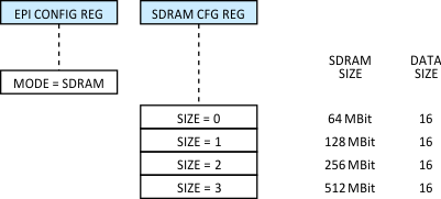 Figure 5-19 EPI SDRAM Mode
Table 5-40 EPI MODES – SDRAM Mode (EPICFG/MODE = 0x1)
| EPI PORT NAME | EPI SIGNAL FUNCTION | DEVICE PIN | |||
|---|---|---|---|---|---|
| ACCESSIBLE BY Cortex-M3 |
ACCESSIBLE BY C28x |
COLUMN/ROW ADDRESS | DATA | (AVAILABLE GPIOMUX_1 MUXING CHOICES FOR EPI) |
|
| EPI0S0 | A0 | D0 | PH3_GPIO51 | ||
| EPI0S1 | A1 | D1 | PH2_GPIO50 | ||
| EPI0S2 | A2 | D2 | PC4_GPIO68 | ||
| EPI0S3 | A3 | D3 | PC5_GPIO69 | ||
| EPI0S4 | A4 | D4 | PC6_GPIO70 | ||
| EPI0S5 | A5 | D5 | PC7_GPIO71 | ||
| EPI0S6 | A6 | D6 | PH0_GPIO48 | ||
| EPI0S7 | A7 | D7 | PH1_GPIO49 | ||
| EPI0S8 | A8 | D8 | PE0_GPIO24 | ||
| EPI0S9 | A9 | D9 | PE1_GPIO25 | ||
| EPI0S10 | A10 | D10 | PH4_GPIO52 | ||
| EPI0S11 | A11 | D11 | PH5_GPIO53 | ||
| EPI0S12 | A12 | D12 | PF4_GPIO36 | ||
| EPI0S13 | BA0 | D13 | PG0_GPIO40 | ||
| EPI0S14 | BA1 | D14 | PG1_GPIO41 | ||
| EPI0S15 | D15 | PF5_GPIO37 | |||
| EPI0S16 | DQML | PJ0_GPIO56 | |||
| EPI0S17 | DQMH | PJ1_GPIO57 | |||
| EPI0S18 | CAS | PJ2_GPIO58 | |||
| EPI0S19 | RAS | PD4_GPIO20 | PJ3_GPIO59 | ||
| EPI0S28 | WE | PD5_GPIO21 | PJ4_GPIO60 | ||
| EPI0S29 | CS | PD6_GPIO22 | PJ5_GPIO61 | ||
| EPI0S30 | CKE | PD7_GPIO23 | PJ6_GPIO62 | ||
| EPI0S31 | CLK | PG7_GPIO47 | |||
| EPI0S20 | x | PD2_GPIO18 | |||
| EPI0S21 | x | PD3_GPIO19 | |||
| EPI0S22 | x | PB5_GPIO13 | |||
| EPI0S23 | x | PB4_GPIO12 | |||
| EPI0S24 | x | PE2_GPIO26 | |||
| EPI0S25 | x | PE3_GPIO27 | |||
| EPI0S26 | x | PH6_GPIO54 | |||
| EPI0S27 | x | PH7_GPIO55 | |||
| EPI0S32 | x | PF2_GPIO34 | PC0_GPIO64 | ||
| EPI0S33 | x | PF3_GPIO35 | PC1_GPIO65 | ||
| EPI0S34 | x | PE4_GPIO28 | |||
| EPI0S35 | x | PE5_GPIO29 | |||
| EPI0S36 | x | PB7_GPIO15 | PC3_GPIO67 | ||
| EPI0S37 | x | PB6_GPIO14 | PC2_GPIO66 | ||
| EPI0S38 | x | PF6_GPIO38 | PE4_GPIO28 | ||
| EPI0S39 | x | PG2_GPIO42 | |||
| EPI0S40 | x | PG5_GPIO45 | |||
| EPI0S41 | x | PG6_GPIO46 | |||
| EPI0S42 | x | PN6_GPIO102 | |||
| EPI0S43 | x | PN7_GPIO103 | |||
5.10.4.3 EPI Host Bus Mode
There are two versions of the EPI Host Bus Mode: an 8-bit version (HB-8) and a 16-bit version (HB-16). Section 5.10.4.3.1 discusses the EPI 8-Bit Host Bus Mode. Section 5.10.4.3.2 discusses the EPI 16-Bit Host Bus Mode.
5.10.4.3.1 EPI 8-Bit Host Bus (HB-8) Mode
The 8-Bit Host Bus (HB-8) Mode uses fewer data pins than the 16-Bit Host Bus (HB-16) Mode; hence, more pins are available for address. The HB-8 Mode is also slower than the General-Purpose Mode in order to accommodate older logic. The HB-8 Mode is selected with the MODE field of EPI Configuration Register. Within the HB-8 Mode, two additional registers are used to select address/data muxing, chip selects, and other options. These registers are the HB-8 Configuration Register and the HB-8 Configuration2 Register. See Figure 5-20 for a snapshot of HB-8 registers, modes, and features.
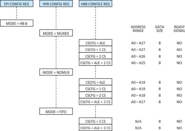 Figure 5-20 EPI 8-Bit Host Bus Mode
5.10.4.3.1.1 HB-8 Muxed Address/Data Mode
The HB-8 Muxed Mode multiplexes address signals with low-order data signals. For this reason, the Muxed Mode allows for a larger address space as compared to the Non-Muxed Mode. The HB-8 Muxed Mode is selected with the MODE field of the HB-8 Configuration Register. In addition to data and address signals, the HB-8 Muxed Mode also features the ALE signal (indicating to an external latch to capture address and hold the address until the data phase); RD and WR data strobes; and 1–4 CS (chip select) signals to enable one of four external peripherals. The ALE and CS options are chosen with the CSCFG field of the HB-8 Configuration2 Register. For more detailed maps of the HB-8 Muxed Mode, see Table 5-41.
Table 5-41 EPI MODES – 8-Bit Host-Bus Mode (EPICFG/MODE = 0x2),
Muxed (EPIHB16CFG/MODE = 0x0)
| EPI PORT NAME | EPI SIGNAL FUNCTION | DEVICE PIN | |||||
|---|---|---|---|---|---|---|---|
| ACCESSIBLE BY Cortex-M3 | ACCESSIBLE BY C28x | WITH ADDRESS LATCH ENABLE (CSCFG = 0x0) |
WITH ONE CHIP SELECT (CSCFG = 0x1) |
WITH TWO CHIP SELECTS (CSCFG = 0x2) |
WITH ALE AND TWO CHIP SELECTS (CSCFG = 0x3) |
(AVAILABLE GPIOMUX_1 MUXING CHOICES FOR EPI) |
|
| EPI0S0 | AD0 | AD0 | AD0 | AD0 | PH3_GPIO51 | ||
| EPI0S1 | AD1 | AD1 | AD1 | AD1 | PH2_GPIO50 | ||
| EPI0S2 | AD2 | AD2 | AD2 | AD2 | PC4_GPIO68 | ||
| EPI0S3 | AD3 | AD3 | AD3 | AD3 | PC5_GPIO69 | ||
| EPI0S4 | AD4 | AD4 | AD4 | AD4 | PC6_GPIO70 | ||
| EPI0S5 | AD5 | AD5 | AD5 | AD5 | PC7_GPIO71 | ||
| EPI0S6 | AD6 | AD6 | AD6 | AD6 | PH0_GPIO48 | ||
| EPI0S7 | AD7 | AD7 | AD7 | AD7 | PH1_GPIO49 | ||
| EPI0S8 | A8 | A8 | A8 | A8 | PE0_GPIO24 | ||
| EPI0S9 | A9 | A9 | A9 | A9 | PE1_GPIO25 | ||
| EPI0S10 | A10 | A10 | A10 | A10 | PH4_GPIO52 | ||
| EPI0S11 | A11 | A11 | A11 | A11 | PH5_GPIO53 | ||
| EPI0S12 | A12 | A12 | A12 | A12 | PF4_GPIO36 | ||
| EPI0S13 | A13 | A13 | A13 | A13 | PG0_GPIO40 | ||
| EPI0S14 | A14 | A14 | A14 | A14 | PG1_GPIO41 | ||
| EPI0S15 | A15 | A15 | A15 | A15 | PF5_GPIO37 | ||
| EPI0S16 | A16 | A16 | A16 | A16 | PJ0_GPIO56 | ||
| EPI0S17 | A17 | A17 | A17 | A17 | PJ1_GPIO57 | ||
| EPI0S18 | A18 | A18 | A18 | A18 | PJ2_GPIO58 | ||
| EPI0S19 | A19 | A19 | A19 | A19 | PD4_GPIO20 | PJ3_GPIO59 | |
| EPI0S20 | A20 | A20 | A20 | A20 | PD2_GPIO18 | ||
| EPI0S21 | A21 | A21 | A21 | A21 | PD3_GPIO19 | ||
| EPI0S22 | A22 | A22 | A22 | A22 | PB5_GPIO13 | ||
| EPI0S23 | A23 | A23 | A23 | A23 | PB4_GPIO12 | ||
| EPI0S24 | A24 | A24 | A24 | A24 | PE2_GPIO26 | ||
| EPI0S25 | A25 | A25 | A25 | A25 | PE3_GPIO27 | ||
| EPI0S26 | A26 | A26 | A26 | CS0 | PH6_GPIO54 | ||
| EPI0S27 | A27 | A27 | CS1 | CS1 | PH7_GPIO55 | ||
| EPI0S30 | ALE | CS0 | CS0 | ALE | PD7_GPIO23 | PJ6_GPIO62 | |
| EPI0S29 | WR | WR | WR | WR | PD6_GPIO22 | PJ5_GPIO61 | |
| EPI0S28 | RD | RD | RD | RD | PD5_GPIO21 | PJ4_GPIO60 | |
| EPI0S31 | x | x | x | x | PG7_GPIO47 | ||
| EPI0S32 | x | x | x | x | PF2_GPIO34 | PC0_GPIO64 | |
| EPI0S33 | x | x | x | x | PF3_GPIO35 | PC1_GPIO65 | |
| EPI0S34 | x | x | x | x | PE4_GPIO28 | ||
| EPI0S35 | x | x | x | x | PE5_GPIO29 | ||
| EPI0S36 | x | x | x | x | PB7_GPIO15 | PC3_GPIO67 | |
| EPI0S37 | x | x | x | x | PB6_GPIO14 | PC2_GPIO66 | |
| EPI0S38 | x | x | x | x | PF6_GPIO38 | PE4_GPIO28 | |
| EPI0S39 | x | x | x | x | PG2_GPIO42 | ||
| EPI0S40 | x | x | x | x | PG5_GPIO45 | ||
| EPI0S41 | x | x | x | x | PG6_GPIO46 | ||
| EPI0S42 | x | x | x | x | PN6_GPIO102 | ||
| EPI0S43 | x | x | x | x | PN7_GPIO103 | ||
5.10.4.3.1.2 HB-8 Non-Muxed Address/Data Mode
The HB-8 Non-Muxed Mode uses dedicated pins for address and data signals. For this reason, the Non-Muxed Mode has reduced address reach as compared to the Muxed Mode. The HB-8 Non-Muxed Mode is selected with the MODE field of the HB-8 Configuration Register. In addition to data and address signals, the HB-8 Non-Muxed Mode also features the ALE signal (indicating to an external latch to capture address and hold the address until the data phase); RD and WR data strobes; and 1–4 CS (chip select) signals to enable one of four external peripherals. The ALE and CS options are chosen with the CSCFG field of the HB-8 Configuration2 Register. For more detailed maps of the HB-8 Non-Muxed Mode, see Table 5-42.
Table 5-42 EPI MODES – 8-Bit Host-Bus Mode (EPICFG/MODE = 0x2),
Non-Muxed (EPIHB16CFG/MODE = 0x1)
| EPI PORT NAME | EPI SIGNAL FUNCTION | DEVICE PIN | |||||
|---|---|---|---|---|---|---|---|
| ACCESSIBLE BY Cortex-M3 | ACCESSIBLE BY C28x | WITH ADDRESS LATCH ENABLE (CSCFG = 0x0) |
WITH ONE CHIP SELECT (CSCFG = 0x1) |
WITH TWO CHIP SELECTS (CSCFG = 0x2) |
WITH ALE AND TWO CHIP SELECTS (CSCFG = 0x3) |
(AVAILABLE GPIOMUX_1 MUXING CHOICES FOR EPI) |
|
| EPI0S0 | D0 | D0 | D0 | D0 | PH3_GPIO51 | ||
| EPI0S1 | D1 | D1 | D1 | D1 | PH2_GPIO50 | ||
| EPI0S2 | D2 | D2 | D2 | D2 | PC4_GPIO68 | ||
| EPI0S3 | D3 | D3 | D3 | D3 | PC5_GPIO69 | ||
| EPI0S4 | D4 | D4 | D4 | D4 | PC6_GPIO70 | ||
| EPI0S5 | D5 | D5 | D5 | D5 | PC7_GPIO71 | ||
| EPI0S6 | D6 | D6 | D6 | D6 | PH0_GPIO48 | ||
| EPI0S7 | D7 | D7 | D7 | D7 | PH1_GPIO49 | ||
| EPI0S8 | A0 | A0 | A0 | A0 | PE0_GPIO24 | ||
| EPI0S9 | A1 | A1 | A1 | A1 | PE1_GPIO25 | ||
| EPI0S10 | A2 | A2 | A2 | A2 | PH4_GPIO52 | ||
| EPI0S11 | A3 | A3 | A3 | A3 | PH5_GPIO53 | ||
| EPI0S12 | A4 | A4 | A4 | A4 | PF4_GPIO36 | ||
| EPI0S13 | A5 | A5 | A5 | A5 | PG0_GPIO40 | ||
| EPI0S14 | A6 | A6 | A6 | A6 | PG1_GPIO41 | ||
| EPI0S15 | A7 | A7 | A7 | A7 | PF5_GPIO37 | ||
| EPI0S16 | A8 | A8 | A8 | A8 | PJ0_GPIO56 | ||
| EPI0S17 | A9 | A9 | A9 | A9 | PJ1_GPIO57 | ||
| EPI0S18 | A10 | A10 | A10 | A10 | PJ2_GPIO58 | ||
| EPI0S19 | A11 | A11 | A11 | A11 | PD4_GPIO20 | PJ3_GPIO59 | |
| EPI0S20 | A12 | A12 | A12 | A12 | PD2_GPIO18 | ||
| EPI0S21 | A13 | A13 | A13 | A13 | PD3_GPIO19 | ||
| EPI0S22 | A14 | A14 | A14 | A14 | PB5_GPIO13 | ||
| EPI0S23 | A15 | A15 | A15 | A15 | PB4_GPIO12 | ||
| EPI0S24 | A16 | A16 | A16 | A16 | PE2_GPIO26 | ||
| EPI0S25 | A17 | A17 | A17 | A17 | PE3_GPIO27 | ||
| EPI0S26 | A18 | A18 | A18 | CS0 | PH6_GPIO54 | ||
| EPI0S27 | A19 | A19 | CS1 | CS1 | PH7_GPIO55 | ||
| EPI0S30 | ALE | CS0 | CS0 | ALE | PD7_GPIO23 | PJ6_GPIO62 | |
| EPI0S29 | WR | WR | WR | WR | PD6_GPIO22 | PJ5_GPIO61 | |
| EPI0S28 | RD | RD | RD | RD | PD5_GPIO21 | PJ4_GPIO60 | |
| EPI0S31 | x | x | x | x | PG7_GPIO47 | ||
| EPI0S32 | x | x | x | x | PF2_GPIO34 | PC0_GPIO64 | |
| EPI0S33 | x | x | x | x | PF3_GPIO35 | PC1_GPIO65 | |
| EPI0S34 | x | x | x | x | PE4_GPIO28 | ||
| EPI0S35 | x | x | x | x | PE5_GPIO29 | ||
| EPI0S36 | x | x | x | x | PB7_GPIO15 | PC3_GPIO67 | |
| EPI0S37 | x | x | x | x | PB6_GPIO14 | PC2_GPIO66 | |
| EPI0S38 | x | x | x | x | PF6_GPIO38 | PE4_GPIO28 | |
| EPI0S39 | x | x | x | x | PG2_GPIO42 | ||
| EPI0S40 | x | x | x | x | PG5_GPIO45 | ||
| EPI0S41 | x | x | x | x | PG6_GPIO46 | ||
| EPI0S42 | x | x | x | x | PN6_GPIO102 | ||
| EPI0S43 | x | x | x | x | PN7_GPIO103 | ||
5.10.4.3.1.3 HB-8 FIFO Mode
The HB-8 FIFO Mode uses 8 bits of data, removes ALE and address pins, and optionally adds external FIFO Full/Empty flag inputs. This scheme is used by many devices, such as radios, communication devices (including USB2 devices), and some FPGA configuration (FIFO through block RAM). This FIFO Mode presents the data side of the normal Host-Bus interface, but is paced by FIFO control signals. It is important to consider that the FIFO Full/Empty control inputs may stall the EPI interface and can potentially block other CPU or DMA accesses. For more detailed maps of the HB-8 FIFO Mode, see Table 5-43.
Table 5-43 EPI MODES – 8-Bit Host-Bus Mode (EPICFG/MODE = 0x2),
FIFO Mode (EPIHB16CFG/MODE = 0x3)
| EPI PORT NAME | EPI SIGNAL FUNCTION | DEVICE PIN | |||
|---|---|---|---|---|---|
| ACCESSIBLE BY Cortex-M3 |
ACCESSIBLE BY C28x |
WITH ONE CHIP SELECT (CSCFG = 0x1) |
WITH TWO CHIP SELECTS (CSCFG = 0x2) |
(AVAILABLE GPIOMUX_1 MUXING CHOICES FOR EPI) |
|
| EPI0S0 | D0 | D0 | PH3_GPIO51 | ||
| EPI0S1 | D1 | D1 | PH2_GPIO50 | ||
| EPI0S2 | D2 | D2 | PC4_GPIO68 | ||
| EPI0S3 | D3 | D3 | PC5_GPIO69 | ||
| EPI0S4 | D4 | D4 | PC6_GPIO70 | ||
| EPI0S5 | D5 | D5 | PC7_GPIO71 | ||
| EPI0S6 | D6 | D6 | PH0_GPIO48 | ||
| EPI0S7 | D7 | D7 | PH1_GPIO49 | ||
| EPI0S25 | x | CS1 | PE3_GPIO27 | ||
| EPI0S30 | CS0 | CS0 | PD7_GPIO23 | PJ6_GPIO62 | |
| EPI0S27 | FFULL | FFULL | PH7_GPIO55 | ||
| EPI0S26 | FEMPTY | FEMPTY | PH6_GPIO54 | ||
| EPI0S29 | WR | WR | PD6_GPIO22 | PJ5_GPIO61 | |
| EPI0S28 | RD | RD | PD5_GPIO21 | PJ4_GPIO60 | |
| EPI0S8 | x | x | PE0_GPIO24 | ||
| EPI0S9 | x | x | PE1_GPIO25 | ||
| EPI0S10 | x | x | PH4_GPIO52 | ||
| EPI0S11 | x | x | PH5_GPIO53 | ||
| EPI0S12 | x | x | PF4_GPIO36 | ||
| EPI0S13 | x | x | PG0_GPIO40 | ||
| EPI0S14 | x | x | PG1_GPIO41 | ||
| EPI0S15 | x | x | PF5_GPIO37 | ||
| EPI0S16 | x | x | PJ0_GPIO56 | ||
| EPI0S17 | x | x | PJ1_GPIO57 | ||
| EPI0S18 | x | x | PJ2_GPIO58 | ||
| EPI0S19 | x | x | PD4_GPIO20 | PJ3_GPIO59 | |
| EPI0S20 | x | x | PD2_GPIO18 | ||
| EPI0S21 | x | x | PD3_GPIO19 | ||
| EPI0S22 | x | x | PB5_GPIO13 | ||
| EPI0S23 | x | x | PB4_GPIO12 | ||
| EPI0S24 | x | x | PE2_GPIO26 | ||
| EPI0S32 | x | x | PF2_GPIO34 | PC0_GPIO64 | |
| EPI0S31 | x | x | PG7_GPIO47 | ||
| EPI0S33 | x | x | PF3_GPIO35 | PC1_GPIO65 | |
| EPI0S34 | x | x | PE4_GPIO28 | ||
| EPI0S35 | x | x | PE5_GPIO29 | ||
| EPI0S36 | x | x | PB7_GPIO15 | PC3_GPIO67 | |
| EPI0S37 | x | x | PB6_GPIO14 | PC2_GPIO66 | |
| EPI0S38 | x | x | PF6_GPIO38 | PE4_GPIO28 | |
| EPI0S39 | x | x | PG2_GPIO42 | ||
| EPI0S40 | x | x | PG5_GPIO45 | ||
| EPI0S41 | x | x | PG6_GPIO46 | ||
| EPI0S42 | x | x | PN6_GPIO102 | ||
| EPI0S43 | x | x | PN7_GPIO103 | ||
5.10.4.3.2 EPI 16-Bit Host Bus (HB-16) Mode
The 16-Bit Host Bus (HB-16) Mode uses fewer address pins than the 8-Bit Host Bus (HB-8) Mode; hence, more pins are available for data. The HB-16 Mode is also slower than the General-Purpose Mode in order to accommodate older logic. The HB-16 Mode is selected with the MODE field of EPI Configuration Register. Within the HB-16 Mode, two additional registers are used to select address/data muxing, byte selects, chip selects, and other options. These registers are the HB-16 Configuration Register and the
HB-16 Configuration2 Register. See Figure 5-21 for a snapshot of HB-16 registers, modes, and features.
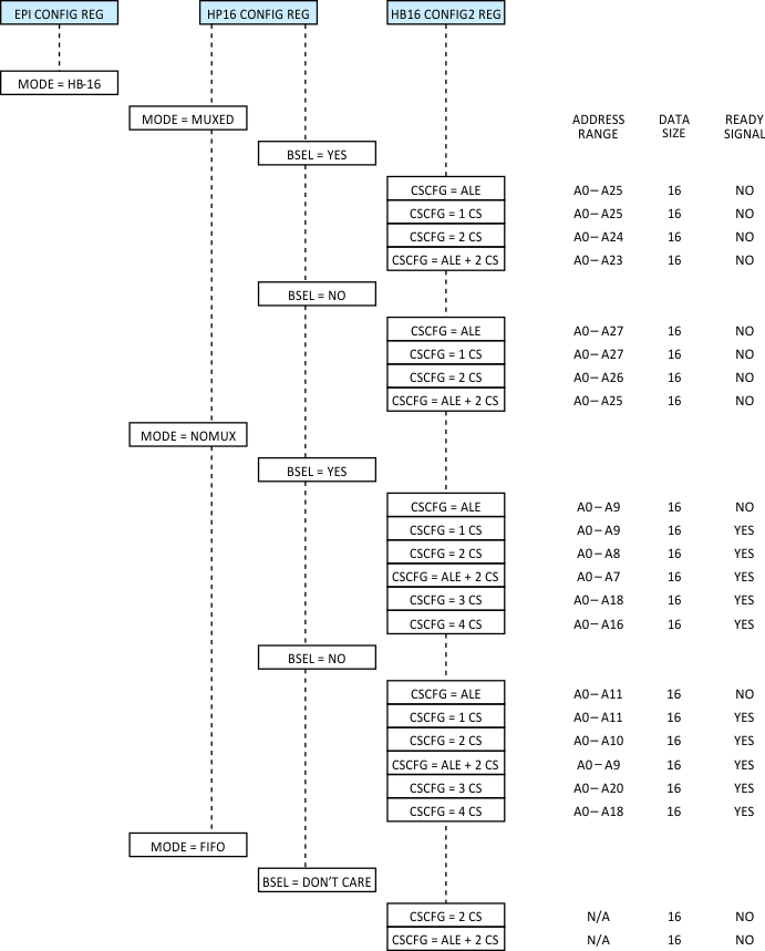 Figure 5-21 EPI 16-Bit Host Bus Mode
5.10.4.3.2.1 HB-16 Muxed Address/Data Mode
The HB-16 Muxed Mode multiplexes address signals with low-order data signals. For this reason, the Muxed Mode allows for a larger address space as compared to the Non-Muxed Mode. The HB-16 Muxed Mode is selected with the MODE field of the HB-16 Configuration Register. In addition to data and address signals, the HB-16 Muxed Mode also features the ALE signal (indicating to an external latch to capture address and hold the address until the data phase); RD and WR data strobes; 1–4 CS (chip select) signals to enable one of four external peripherals; and two BSEL (byte select) signals to accommodate byte accesses to lower or upper half of 16-bit data. The Byte Selects are chosen with the BSEL field of the HB-16 Configuration Register. The ALE and CS options are chosen with the CSCFG field of the HB-16 Configuration2 Register. For more detailed maps of the HB-16 Muxed Mode without Byte Selects, see Table 5-44. For more detailed maps of the HB-16 Muxed Mode with Byte Selects, see Table 5-45.
Table 5-44 EPI MODES – 16-Bit Host-Bus Mode (EPICFG/MODE = 0x3),
Muxed (EPIHB16CFG/MODE = 0x0), Without Byte Selects (EPIHB16CFG/BSEL = 0x1),
and With Chip Selects (EPIHB16CFG2/CSCFG = 0x0,1,2,3)
| EPI PORT NAME | EPI SIGNAL FUNCTION | DEVICE PIN | |||||
|---|---|---|---|---|---|---|---|
| ACCESSIBLE BY Cortex-M3 | ACCESSIBLE BY C28x | WITH ADDRESS LATCH ENABLE (CSCFG = 0x0) |
WITH ONE CHIP SELECT (CSCFG = 0x1) |
WITH TWO CHIP SELECTS (CSCFG = 0x2) |
WITH ALE AND TWO CHIP SELECTS (CSCFG = 0x3) |
(AVAILABLE GPIOMUX_1 MUXING CHOICES FOR EPI) |
|
| EPI0S0 | AD0 | AD0 | AD0 | AD0 | PH3_GPIO51 | ||
| EPI0S1 | AD1 | AD1 | AD1 | AD1 | PH2_GPIO50 | ||
| EPI0S2 | AD2 | AD2 | AD2 | AD2 | PC4_GPIO68 | ||
| EPI0S3 | AD3 | AD3 | AD3 | AD3 | PC5_GPIO69 | ||
| EPI0S4 | AD4 | AD4 | AD4 | AD4 | PC6_GPIO70 | ||
| EPI0S5 | AD5 | AD5 | AD5 | AD5 | PC7_GPIO71 | ||
| EPI0S6 | AD6 | AD6 | AD6 | AD6 | PH0_GPIO48 | ||
| EPI0S7 | AD7 | AD7 | AD7 | AD7 | PH1_GPIO49 | ||
| EPI0S8 | AD8 | AD8 | AD8 | AD8 | PE0_GPIO24 | ||
| EPI0S9 | AD9 | AD9 | AD9 | AD9 | PE1_GPIO25 | ||
| EPI0S10 | AD10 | AD10 | AD10 | AD10 | PH4_GPIO52 | ||
| EPI0S11 | AD11 | AD11 | AD11 | AD11 | PH5_GPIO53 | ||
| EPI0S12 | AD12 | AD12 | AD12 | AD12 | PF4_GPIO36 | ||
| EPI0S13 | AD13 | AD13 | AD13 | AD13 | PG0_GPIO40 | ||
| EPI0S14 | AD14 | AD14 | AD14 | AD14 | PG1_GPIO41 | ||
| EPI0S15 | AD15 | AD15 | AD15 | AD15 | PF5_GPIO37 | ||
| EPI0S16 | A16 | A16 | A16 | A16 | PJ0_GPIO56 | ||
| EPI0S17 | A17 | A17 | A17 | A17 | PJ1_GPIO57 | ||
| EPI0S18 | A18 | A18 | A18 | A18 | PJ2_GPIO58 | ||
| EPI0S19 | A19 | A19 | A19 | A19 | PD4_GPIO20 | PJ3_GPIO59 | |
| EPI0S20 | A20 | A20 | A20 | A20 | PD2_GPIO18 | ||
| EPI0S21 | A21 | A21 | A21 | A21 | PD3_GPIO19 | ||
| EPI0S22 | A22 | A22 | A22 | A22 | PB5_GPIO13 | ||
| EPI0S23 | A23 | A23 | A23 | A23 | PB4_GPIO12 | ||
| EPI0S24 | A24 | A24 | A24 | A24 | PE2_GPIO26 | ||
| EPI0S25 | A25 | A25 | A25 | A25 | PE3_GPIO27 | ||
| EPI0S26 | A26 | A26 | A26 | CS0 | PH6_GPIO54 | ||
| EPI0S27 | A27 | A27 | CS1 | CS1 | PH7_GPIO55 | ||
| EPI0S30 | ALE | CS0 | CS0 | ALE | PD7_GPIO23 | PJ6_GPIO62 | |
| EPI0S29 | WR | WR | WR | WR | PD6_GPIO22 | PJ5_GPIO61 | |
| EPI0S28 | RD | RD | RD | RD | PD5_GPIO21 | PJ4_GPIO60 | |
| EPI0S31 | x | x | x | x | PG7_GPIO47 | ||
| EPI0S32 | x | x | x | x | PF2_GPIO34 | PC0_GPIO64 | |
| EPI0S33 | x | x | x | x | PF3_GPIO35 | PC1_GPIO65 | |
| EPI0S34 | x | x | x | x | PE4_GPIO28 | ||
| EPI0S35 | x | x | x | x | PE5_GPIO29 | ||
| EPI0S36 | x | x | x | x | PB7_GPIO15 | PC3_GPIO67 | |
| EPI0S37 | x | x | x | x | PB6_GPIO14 | PC2_GPIO66 | |
| EPI0S38 | x | x | x | x | PF6_GPIO38 | PE4_GPIO28 | |
| EPI0S39 | x | x | x | x | PG2_GPIO42 | ||
| EPI0S40 | x | x | x | x | PG5_GPIO45 | ||
| EPI0S41 | x | x | x | x | PG6_GPIO46 | ||
| EPI0S42 | x | x | x | x | PN6_GPIO102 | ||
| EPI0S43 | x | x | x | x | PN7_GPIO103 | ||
Table 5-45 EPI MODES – 16-Bit Host-Bus (EPICFG/MODE = 0x3),
Muxed (EPIHB16CFG/MODE = 0x0), With Byte Selects (EPIHB16CFG/BSEL = 0x0),
and With Chip Selects (EPIHB16CFG2/CSCFG=0x0,1,2,3)
| EPI PORT NAME | EPI SIGNAL FUNCTION | DEVICE PIN | |||||
|---|---|---|---|---|---|---|---|
| ACCESSIBLE BY Cortex-M3 | ACCESSIBLE BY C28x | WITH ADDRESS LATCH ENABLE (CSCFG = 0x0) |
WITH ONE CHIP SELECT (CSCFG = 0x1) |
WITH TWO CHIP SELECTS (CSCFG = 0x2) |
WITH ALE AND TWO CHIP SELECTS (CSCFG = 0x3) |
(AVAILABLE GPIOMUX_1 MUXING CHOICES FOR EPI) |
|
| EPI0S0 | AD0 | AD0 | AD0 | AD0 | PH3_GPIO51 | ||
| EPI0S1 | AD1 | AD1 | AD1 | AD1 | PH2_GPIO50 | ||
| EPI0S2 | AD2 | AD2 | AD2 | AD2 | PC4_GPIO68 | ||
| EPI0S3 | AD3 | AD3 | AD3 | AD3 | PC5_GPIO69 | ||
| EPI0S4 | AD4 | AD4 | AD4 | AD4 | PC6_GPIO70 | ||
| EPI0S5 | AD5 | AD5 | AD5 | AD5 | PC7_GPIO71 | ||
| EPI0S6 | AD6 | AD6 | AD6 | AD6 | PH0_GPIO48 | ||
| EPI0S7 | AD7 | AD7 | AD7 | AD7 | PH1_GPIO49 | ||
| EPI0S8 | AD8 | AD8 | AD8 | AD8 | PE0_GPIO24 | ||
| EPI0S9 | AD9 | AD9 | AD9 | AD9 | PE1_GPIO25 | ||
| EPI0S10 | AD10 | AD10 | AD10 | AD10 | PH4_GPIO52 | ||
| EPI0S11 | AD11 | AD11 | AD11 | AD11 | PH5_GPIO53 | ||
| EPI0S12 | AD12 | AD12 | AD12 | AD12 | PF4_GPIO36 | ||
| EPI0S13 | AD13 | AD13 | AD13 | AD13 | PG0_GPIO40 | ||
| EPI0S14 | AD14 | AD14 | AD14 | AD14 | PG1_GPIO41 | ||
| EPI0S15 | AD15 | AD15 | AD15 | AD15 | PF5_GPIO37 | ||
| EPI0S16 | A16 | A16 | A16 | A16 | PJ0_GPIO56 | ||
| EPI0S17 | A17 | A17 | A17 | A17 | PJ1_GPIO57 | ||
| EPI0S18 | A18 | A18 | A18 | A18 | PJ2_GPIO58 | ||
| EPI0S19 | A19 | A19 | A19 | A19 | PD4_GPIO20 | PJ3_GPIO59 | |
| EPI0S20 | A20 | A20 | A20 | A20 | PD2_GPIO18 | ||
| EPI0S21 | A21 | A21 | A21 | A21 | PD3_GPIO19 | ||
| EPI0S22 | A22 | A22 | A22 | A22 | PB5_GPIO13 | ||
| EPI0S23 | A23 | A23 | A23 | A23 | PB4_GPIO12 | ||
| EPI0S24 | A24 | A24 | A24 | BSEL0 | PE2_GPIO26 | ||
| EPI0S25 | A25 | A25 | BSEL0 | BSEL1 | PE3_GPIO27 | ||
| EPI0S26 | BSEL0 | BSEL0 | BSEL1 | CS0 | PH6_GPIO54 | ||
| EPI0S27 | BSEL1 | BSEL1 | CS1 | CS1 | PH7_GPIO55 | ||
| EPI0S30 | ALE | CS0 | CS0 | ALE | PD7_GPIO23 | PJ6_GPIO62 | |
| EPI0S29 | WR | WR | WR | WR | PD6_GPIO22 | PJ5_GPIO61 | |
| EPI0S28 | RD | RD | RD | RD | PD5_GPIO21 | PJ4_GPIO60 | |
| EPI0S31 | x | x | x | x | PG7_GPIO47 | ||
| EPI0S32 | x | x | x | x | PF2_GPIO34 | PC0_GPIO64 | |
| EPI0S33 | x | x | x | x | PF3_GPIO35 | PC1_GPIO65 | |
| EPI0S34 | x | x | x | x | PE4_GPIO28 | ||
| EPI0S35 | x | x | x | x | PE5_GPIO29 | ||
| EPI0S36 | x | x | x | x | PB7_GPIO15 | PC3_GPIO67 | |
| EPI0S37 | x | x | x | x | PB6_GPIO14 | PC2_GPIO66 | |
| EPI0S38 | x | x | x | x | PF6_GPIO38 | PE4_GPIO28 | |
| EPI0S39 | x | x | x | x | PG2_GPIO42 | ||
| EPI0S40 | x | x | x | x | PG5_GPIO45 | ||
| EPI0S41 | x | x | x | x | PG6_GPIO46 | ||
| EPI0S42 | x | x | x | x | PN6_GPIO102 | ||
| EPI0S43 | x | x | x | x | PN7_GPIO103 | ||
5.10.4.3.2.2 HB-16 Non-Muxed Address/Data Mode
The HB-16 Non-Muxed Mode uses dedicated pins for address and data signals. For this reason, the Non-Muxed Mode has reduced address reach as compared to the Muxed Mode. The HB-16 Non-Muxed Mode is selected with the MODE field of the HB-16 Configuration Register. In addition to data and address signals, the HB-16 Non-Muxed Mode also features the ALE signal (indicating to an external latch to capture address and hold the address until the data phase); RD and WR data strobes; 1–4 CS (chip select) signals to enable one of four external peripherals; and two BSEL (byte select) signals to accommodate byte accesses to lower or upper half of 16-bit data. The Byte Selects are chosen with the BSEL field of the HB-16 Configuration Register. The ALE and CS options are chosen with the CSCFG field of the HB-16 Configuration2 Register. For Non-Muxed bus cycles, most of the CSCFG modes also support a RDY signal. The RDY input to EPI is used by an external peripheral to extend bus cycles when the peripheral needs more time to complete reading or writing of data. While most EPI modes use up to 32 pins, the Non-Muxed CSCFG modes with 3 and 4 Chip Selects use 12 additional pins to extend the address reach and the number of CS signals. For detailed maps of HB-16 Non-Muxed Modes without Byte Selects, see Table 5-46 and Table 5-47. For detailed maps of HB-16 Non-Muxed Modes with Byte Selects, see Table 5-48 and Table 5-49.
Table 5-46 EPI MODES – 16-Bit Host-Bus Mode (EPICFG/MODE = 0x3),
Non-Muxed (EPIHB16CFG/MODE = 0x1), Without Byte Selects (EPIHB16CFG/BSEL = 0x1),
and With Chip Selects (EPIHB16CFG2/CSCFG = 0x0,1,2,3)
| EPI PORT NAME | EPI SIGNAL FUNCTION | DEVICE PIN | |||||
|---|---|---|---|---|---|---|---|
| ACCESSIBLE BY Cortex-M3 | ACCESSIBLE BY C28x | WITH ADDRESS LATCH ENABLE (CSCFG = 0x0) |
WITH ONE CHIP SELECT (CSCFG = 0x1) |
WITH TWO CHIP SELECTS (CSCFG = 0x2) |
WITH ALE AND TWO CHIP SELECTS (CSCFG = 0x3) |
(AVAILABLE GPIOMUX_1 MUXING CHOICES FOR EPI) |
|
| EPI0S0 | D0 | D0 | D0 | D0 | PH3_GPIO51 | ||
| EPI0S1 | D1 | D1 | D1 | D1 | PH2_GPIO50 | ||
| EPI0S2 | D2 | D2 | D2 | D2 | PC4_GPIO68 | ||
| EPI0S3 | D3 | D3 | D3 | D3 | PC5_GPIO69 | ||
| EPI0S4 | D4 | D4 | D4 | D4 | PC6_GPIO70 | ||
| EPI0S5 | D5 | D5 | D5 | D5 | PC7_GPIO71 | ||
| EPI0S6 | D6 | D6 | D6 | D6 | PH0_GPIO48 | ||
| EPI0S7 | D7 | D7 | D7 | D7 | PH1_GPIO49 | ||
| EPI0S8 | D8 | D8 | D8 | D8 | PE0_GPIO24 | ||
| EPI0S9 | D9 | D9 | D9 | D9 | PE1_GPIO25 | ||
| EPI0S10 | D10 | D10 | D10 | D10 | PH4_GPIO52 | ||
| EPI0S11 | D11 | D11 | D11 | D11 | PH5_GPIO53 | ||
| EPI0S12 | D12 | D12 | D12 | D12 | PF4_GPIO36 | ||
| EPI0S13 | D13 | D13 | D13 | D13 | PG0_GPIO40 | ||
| EPI0S14 | D14 | D14 | D14 | D14 | PG1_GPIO41 | ||
| EPI0S15 | D15 | D15 | D15 | D15 | PF5_GPIO37 | ||
| EPI0S16 | A0 | A0 | A0 | A0 | PJ0_GPIO56 | ||
| EPI0S17 | A1 | A1 | A1 | A1 | PJ1_GPIO57 | ||
| EPI0S18 | A2 | A2 | A2 | A2 | PJ2_GPIO58 | ||
| EPI0S19 | A3 | A3 | A3 | A3 | PD4_GPIO20 | PJ3_GPIO59 | |
| EPI0S20 | A4 | A4 | A4 | A4 | PD2_GPIO18 | ||
| EPI0S21 | A5 | A5 | A5 | A5 | PD3_GPIO19 | ||
| EPI0S22 | A6 | A6 | A6 | A6 | PB5_GPIO13 | ||
| EPI0S23 | A7 | A7 | A7 | A7 | PB4_GPIO12 | ||
| EPI0S24 | A8 | A8 | A8 | A8 | PE2_GPIO26 | ||
| EPI0S25 | A9 | A9 | A9 | A9 | PE3_GPIO27 | ||
| EPI0S26 | A10 | A10 | A10 | CS0 | PH6_GPIO54 | ||
| EPI0S27 | A11 | A11 | CS1 | CS1 | PH7_GPIO55 | ||
| EPI0S30 | ALE | CS0 | CS0 | ALE | PD7_GPIO23 | PJ6_GPIO62 | |
| EPI0S29 | WR | WR | WR | WR | PD6_GPIO22 | PJ5_GPIO61 | |
| EPI0S28 | RD | RD | RD | RD | PD5_GPIO21 | PJ4_GPIO60 | |
| EPI0S32 | x | RDY | RDY | RDY | PF2_GPIO34 | PC0_GPIO64 | |
| EPI0S31 | x | x | x | x | PG7_GPIO47 | ||
| EPI0S33 | x | x | x | x | PF3_GPIO35 | PC1_GPIO65 | |
| EPI0S34 | x | x | x | x | PE4_GPIO28 | ||
| EPI0S35 | x | x | x | x | PE5_GPIO29 | ||
| EPI0S36 | x | x | x | x | PB7_GPIO15 | PC3_GPIO67 | |
| EPI0S37 | x | x | x | x | PB6_GPIO14 | PC2_GPIO66 | |
| EPI0S38 | x | x | x | x | PF6_GPIO38 | PE4_GPIO28 | |
| EPI0S39 | x | x | x | x | PG2_GPIO42 | ||
| EPI0S40 | x | x | x | x | PG5_GPIO45 | ||
| EPI0S41 | x | x | x | x | PG6_GPIO46 | ||
| EPI0S42 | x | x | x | x | PN6_GPIO102 | ||
| EPI0S43 | x | x | x | x | PN7_GPIO103 | ||
Table 5-47 EPI MODES – 16-Bit Host-Bus Mode (EPICFG/MODE=0x3),
Non-Muxed (EPIHB16CFG/MODE = 0x1), Without Byte Selects (EPIHB16CFG/BSEL = 0x1),
and With Additional Chip Selects (EPIHB16CFG2/CSCFG = 0x5,7)
| EPI PORT NAME | EPI SIGNAL FUNCTION | DEVICE PIN | EPI PORT NAME | EPI SIGNAL FUNCTION | DEVICE PIN | |||||
|---|---|---|---|---|---|---|---|---|---|---|
| ACCESSIBLE BY Cortex-M3 |
ACCESSIBLE BY C28x |
WITH THREE CHIP SELECTS (CSCFG = 0x7) |
(AVAILABLE GPIOMUX_1 MUXING CHOICES FOR EPI) |
ACCESSIBLE BY Cortex-M3 |
ACCESSIBLE BY C28x |
WITH FOUR CHIP SELECTS (CSCFG = 0x5) |
(AVAILABLE GPIOMUX_1 MUXING CHOICES FOR EPI) |
|||
| EPI0S0 | D0 | PH3_GPIO51 | EPI0S0 | D0 | PH3_GPIO51 | |||||
| EPI0S1 | D1 | PH2_GPIO50 | EPI0S1 | D1 | PH2_GPIO50 | |||||
| EPI0S2 | D2 | PC4_GPIO68 | EPI0S2 | D2 | PC4_GPIO68 | |||||
| EPI0S3 | D3 | PC5_GPIO69 | EPI0S3 | D3 | PC5_GPIO69 | |||||
| EPI0S4 | D4 | PC6_GPIO70 | EPI0S4 | D4 | PC6_GPIO70 | |||||
| EPI0S5 | D5 | PC7_GPIO71 | EPI0S5 | D5 | PC7_GPIO71 | |||||
| EPI0S6 | D6 | PH0_GPIO48 | EPI0S6 | D6 | PH0_GPIO48 | |||||
| EPI0S7 | D7 | PH1_GPIO49 | EPI0S7 | D7 | PH1_GPIO49 | |||||
| EPI0S8 | D8 | PE0_GPIO24 | EPI0S8 | D8 | PE0_GPIO24 | |||||
| EPI0S9 | D9 | PE1_GPIO25 | EPI0S9 | D9 | PE1_GPIO25 | |||||
| EPI0S10 | D10 | PH4_GPIO52 | EPI0S10 | D10 | PH4_GPIO52 | |||||
| EPI0S11 | D11 | PH5_GPIO53 | EPI0S11 | D11 | PH5_GPIO53 | |||||
| EPI0S12 | D12 | PF4_GPIO36 | EPI0S12 | D12 | PF4_GPIO36 | |||||
| EPI0S13 | D13 | PG0_GPIO40 | EPI0S13 | D13 | PG0_GPIO40 | |||||
| EPI0S14 | D14 | PG1_GPIO41 | EPI0S14 | D14 | PG1_GPIO41 | |||||
| EPI0S15 | D15 | PF5_GPIO37 | EPI0S15 | D15 | PF5_GPIO37 | |||||
| EPI0S16 | A0 | PJ0_GPIO56 | EPI0S16 | A0 | PJ0_GPIO56 | |||||
| EPI0S17 | A1 | PJ1_GPIO57 | EPI0S17 | A1 | PJ1_GPIO57 | |||||
| EPI0S18 | A2 | PJ2_GPIO58 | EPI0S18 | A2 | PJ2_GPIO58 | |||||
| EPI0S19 | A3 | PD4_GPIO20 | PJ3_GPIO59 | EPI0S19 | A3 | PD4_GPIO20 | PJ3_GPIO59 | |||
| EPI0S20 | A4 | PD2_GPIO18 | EPI0S20 | A4 | PD2_GPIO18 | |||||
| EPI0S21 | A5 | PD3_GPIO19 | EPI0S21 | A5 | PD3_GPIO19 | |||||
| EPI0S22 | A6 | PB5_GPIO13 | EPI0S22 | A6 | PB5_GPIO13 | |||||
| EPI0S23 | A7 | PB4_GPIO12 | EPI0S23 | A7 | PB4_GPIO12 | |||||
| EPI0S24 | A8 | PE2_GPIO26 | EPI0S24 | A8 | PE2_GPIO26 | |||||
| EPI0S25 | A9 | PE3_GPIO27 | EPI0S25 | A9 | PE3_GPIO27 | |||||
| EPI0S26 | A10 | PH6_GPIO54 | EPI0S26 | A10 | PH6_GPIO54 | |||||
| EPI0S36 | A11 | PB7_GPIO15 | PC3_GPIO67 | EPI0S36 | A11 | PB7_GPIO15 | PC3_GPIO67 | |||
| EPI0S37 | A12 | PB6_GPIO14 | PC2_GPIO66 | EPI0S37 | A12 | PB6_GPIO14 | PC2_GPIO66 | |||
| EPI0S38 | A13 | PF6_GPIO38 | PE4_GPIO28 | EPI0S38 | A13 | PF6_GPIO38 | PE4_GPIO28 | |||
| EPI0S39 | A14 | PG2_GPIO42 | EPI0S39 | A14 | PG2_GPIO42 | |||||
| EPI0S27 | A15 | PH7_GPIO55 | EPI0S40 | A15 | PG5_GPIO45 | |||||
| EPI0S35 | A16 | PE5_GPIO29 | EPI0S41 | A16 | PG6_GPIO46 | |||||
| EPI0S40 | A17 | PG5_GPIO45 | EPI0S42 | A17 | PN6_GPIO102 | |||||
| EPI0S41 | A18 | PG6_GPIO46 | EPI0S43 | A18 | PN7_GPIO103 | |||||
| EPI0S42 | A19 | PN6_GPIO102 | EPI0S30 | CS0 | PD7_GPIO23 | PJ6_GPIO62 | ||||
| EPI0S43 | A20 | PN7_GPIO103 | EPI0S27 | CS1 | PH7_GPIO55 | |||||
| EPI0S30 | CS0 | PD7_GPIO23 | PJ6_GPIO62 | EPI0S34 | CS2 | PE4_GPIO28 | ||||
| EPI0S34 | CS2 | PE4_GPIO28 | EPI0S33 | CS3 | PF3_GPIO35 | PC1_GPIO65 | ||||
| EPI0S33 | CS3 | PF3_GPIO35 | PC1_GPIO65 | |||||||
| EPI0S29 | WR | PD6_GPIO22 | PJ5_GPIO61 | |||||||
| EPI0S29 | WR | PD6_GPIO22 | PJ5_GPIO61 | EPI0S28 | RD | PD5_GPIO21 | PJ4_GPIO60 | |||
| EPI0S28 | RD | PD5_GPIO21 | PJ4_GPIO60 | EPI0S32 | RDY | PF2_GPIO34 | PC0_GPIO64 | |||
| EPI0S32 | RDY | PF2_GPIO34 | PC0_GPIO64 | |||||||
| EPI0S31 | x | PG7_GPIO47 | ||||||||
| EPI0S31 | x | PG7_GPIO47 | EPI0S35 | x | PE5_GPIO29 | |||||
Table 5-48 EPI MODES – 16-Bit Host-Bus (EPICFG/MODE = 0x3),
Non-Muxed (EPIHB16CFG/MODE = 0x1), With Byte Selects (EPIHB16CFG/BSEL = 0x0),
and With Chip Selects (EPIHB16CFG2/CSCFG = 0x0,1,2,3)
| EPI PORT NAME | EPI SIGNAL FUNCTION | DEVICE PIN | |||||
|---|---|---|---|---|---|---|---|
| ACCESSIBLE BY Cortex-M3 | ACCESSIBLE BY C28x | WITH ADDRESS LATCH ENABLE (CSCFG = 0x0) |
WITH ONE CHIP SELECT (CSCFG = 0x1) |
WITH TWO CHIP SELECTS (CSCFG = 0x2) |
WITH ALE AND TWO CHIP SELECTS (CSCFG = 0x3) |
(AVAILABLE GPIOMUX_1 MUXING CHOICES FOR EPI) |
|
| EPI0S0 | D0 | D0 | D0 | D0 | PH3_GPIO51 | ||
| EPI0S1 | D1 | D1 | D1 | D1 | PH2_GPIO50 | ||
| EPI0S2 | D2 | D2 | D2 | D2 | PC4_GPIO68 | ||
| EPI0S3 | D3 | D3 | D3 | D3 | PC5_GPIO69 | ||
| EPI0S4 | D4 | D4 | D4 | D4 | PC6_GPIO70 | ||
| EPI0S5 | D5 | D5 | D5 | D5 | PC7_GPIO71 | ||
| EPI0S6 | D6 | D6 | D6 | D6 | PH0_GPIO48 | ||
| EPI0S7 | D7 | D7 | D7 | D7 | PH1_GPIO49 | ||
| EPI0S8 | D8 | D8 | D8 | D8 | PE0_GPIO24 | ||
| EPI0S9 | D9 | D9 | D9 | D9 | PE1_GPIO25 | ||
| EPI0S10 | D10 | D10 | D10 | D10 | PH4_GPIO52 | ||
| EPI0S11 | D11 | D11 | D11 | D11 | PH5_GPIO53 | ||
| EPI0S12 | D12 | D12 | D12 | D12 | PF4_GPIO36 | ||
| EPI0S13 | D13 | D13 | D13 | D13 | PG0_GPIO40 | ||
| EPI0S14 | D14 | D14 | D14 | D14 | PG1_GPIO41 | ||
| EPI0S15 | D15 | D15 | D15 | D15 | PF5_GPIO37 | ||
| EPI0S16 | A0 | A0 | A0 | A0 | PJ0_GPIO56 | ||
| EPI0S17 | A1 | A1 | A1 | A1 | PJ1_GPIO57 | ||
| EPI0S18 | A2 | A2 | A2 | A2 | PJ2_GPIO58 | ||
| EPI0S19 | A3 | A3 | A3 | A3 | PD4_GPIO20 | PJ3_GPIO59 | |
| EPI0S20 | A4 | A4 | A4 | A4 | PD2_GPIO18 | ||
| EPI0S21 | A5 | A5 | A5 | A5 | PD3_GPIO19 | ||
| EPI0S22 | A6 | A6 | A6 | A6 | PB5_GPIO13 | ||
| EPI0S23 | A7 | A7 | A7 | A7 | PB4_GPIO12 | ||
| EPI0S24 | A8 | A8 | A8 | BSEL0 | PE2_GPIO26 | ||
| EPI0S25 | A9 | A9 | BSEL0 | BSEL1 | PE3_GPIO27 | ||
| EPI0S26 | BSEL0 | BSEL0 | BSEL1 | CS0 | PH6_GPIO54 | ||
| EPI0S27 | BSEL1 | BSEL1 | CS1 | CS1 | PH7_GPIO55 | ||
| EPI0S30 | ALE | CS0 | CS0 | ALE | PD7_GPIO23 | PJ6_GPIO62 | |
| EPI0S29 | WR | WR | WR | WR | PD6_GPIO22 | PJ5_GPIO61 | |
| EPI0S28 | RD | RD | RD | RD | PD5_GPIO21 | PJ4_GPIO60 | |
| EPI0S32 | x | RDY | RDY | RDY | PF2_GPIO34 | PC0_GPIO64 | |
| EPI0S31 | x | x | x | x | PG7_GPIO47 | ||
| EPI0S33 | x | x | x | x | PF3_GPIO35 | PC1_GPIO65 | |
| EPI0S34 | x | x | x | x | PE4_GPIO28 | ||
| EPI0S35 | x | x | x | x | PE5_GPIO29 | ||
| EPI0S36 | x | x | x | x | PB7_GPIO15 | PC3_GPIO67 | |
| EPI0S37 | x | x | x | x | PB6_GPIO14 | PC2_GPIO66 | |
| EPI0S38 | x | x | x | x | PF6_GPIO38 | PE4_GPIO28 | |
| EPI0S39 | x | x | x | x | PG2_GPIO42 | ||
| EPI0S40 | x | x | x | x | PG5_GPIO45 | ||
| EPI0S41 | x | x | x | x | PG6_GPIO46 | ||
| EPI0S42 | x | x | x | x | PN6_GPIO102 | ||
| EPI0S43 | x | x | x | x | PN7_GPIO103 | ||
Table 5-49 EPI MODES – 16-Bit Host-Bus (EPICFG/MODE = 0x3),
Non-Muxed (EPIHB16CFG/MODE = 0x1), With Byte Selects (EPIHB16CFG/BSEL = 0x0),
and With Additional Chip Selects (EPIHB16CFG2/CSCFG = 0x5,7)
| EPI PORT NAME | EPI SIGNAL FUNCTION | DEVICE PIN | EPI PORT NAME | EPI SIGNAL FUNCTION | DEVICE PIN | |||||
|---|---|---|---|---|---|---|---|---|---|---|
| ACCESSIBLE BY Cortex-M3 |
ACCESSIBLE BY C28x |
WITH THREE CHIP SELECTS (CSCFG = 0x7) |
(AVAILABLE GPIOMUX_1 MUXING CHOICES FOR EPI) |
ACCESSIBLE BY Cortex-M3 |
ACCESSIBLE BY C28x |
WITH FOUR CHIP SELECTS (CSCFG = 0x5) |
(AVAILABLE GPIOMUX_1 MUXING CHOICES FOR EPI) |
|||
| EPI0S0 | D0 | PH3_GPIO51 | EPI0S0 | D0 | PH3_GPIO51 | |||||
| EPI0S1 | D1 | PH2_GPIO50 | EPI0S1 | D1 | PH2_GPIO50 | |||||
| EPI0S2 | D2 | PC4_GPIO68 | EPI0S2 | D2 | PC4_GPIO68 | |||||
| EPI0S3 | D3 | PC5_GPIO69 | EPI0S3 | D3 | PC5_GPIO69 | |||||
| EPI0S4 | D4 | PC6_GPIO70 | EPI0S4 | D4 | PC6_GPIO70 | |||||
| EPI0S5 | D5 | PC7_GPIO71 | EPI0S5 | D5 | PC7_GPIO71 | |||||
| EPI0S6 | D6 | PH0_GPIO48 | EPI0S6 | D6 | PH0_GPIO48 | |||||
| EPI0S7 | D7 | PH1_GPIO49 | EPI0S7 | D7 | PH1_GPIO49 | |||||
| EPI0S8 | D8 | PE0_GPIO24 | EPI0S8 | D8 | PE0_GPIO24 | |||||
| EPI0S9 | D9 | PE1_GPIO25 | EPI0S9 | D9 | PE1_GPIO25 | |||||
| EPI0S10 | D10 | PH4_GPIO52 | EPI0S10 | D10 | PH4_GPIO52 | |||||
| EPI0S11 | D11 | PH5_GPIO53 | EPI0S11 | D11 | PH5_GPIO53 | |||||
| EPI0S12 | D12 | PF4_GPIO36 | EPI0S12 | D12 | PF4_GPIO36 | |||||
| EPI0S13 | D13 | PG0_GPIO40 | EPI0S13 | D13 | PG0_GPIO40 | |||||
| EPI0S14 | D14 | PG1_GPIO41 | EPI0S14 | D14 | PG1_GPIO41 | |||||
| EPI0S15 | D15 | PF5_GPIO37 | EPI0S15 | D15 | PF5_GPIO37 | |||||
| EPI0S16 | A0 | PJ0_GPIO56 | EPI0S16 | A0 | PJ0_GPIO56 | |||||
| EPI0S17 | A1 | PJ1_GPIO57 | EPI0S17 | A1 | PJ1_GPIO57 | |||||
| EPI0S18 | A2 | PJ2_GPIO58 | EPI0S18 | A2 | PJ2_GPIO58 | |||||
| EPI0S19 | A3 | PD4_GPIO20 | PJ3_GPIO59 | EPI0S19 | A3 | PD4_GPIO20 | PJ3_GPIO59 | |||
| EPI0S20 | A4 | PD2_GPIO18 | EPI0S20 | A4 | PD2_GPIO18 | |||||
| EPI0S21 | A5 | PD3_GPIO19 | EPI0S21 | A5 | PD3_GPIO19 | |||||
| EPI0S22 | A6 | PB5_GPIO13 | EPI0S22 | A6 | PB5_GPIO13 | |||||
| EPI0S23 | A7 | PB4_GPIO12 | EPI0S23 | A7 | PB4_GPIO12 | |||||
| EPI0S24 | A8 | PE2_GPIO26 | EPI0S24 | A8 | PE2_GPIO26 | |||||
| EPI0S40 | A9 | PG5_GPIO45 | EPI0S40 | A9 | PG5_GPIO45 | |||||
| EPI0S41 | A10 | PG6_GPIO46 | EPI0S41 | A10 | PG6_GPIO46 | |||||
| EPI0S36 | A11 | PB7_GPIO15 | PC3_GPIO67 | EPI0S36 | A11 | PB7_GPIO15 | PC3_GPIO67 | |||
| EPI0S37 | A12 | PB6_GPIO14 | PC2_GPIO66 | EPI0S37 | A12 | PB6_GPIO14 | PC2_GPIO66 | |||
| EPI0S38 | A13 | PF6_GPIO38 | PE4_GPIO28 | EPI0S38 | A13 | PF6_GPIO38 | PE4_GPIO28 | |||
| EPI0S39 | A14 | PG2_GPIO42 | EPI0S39 | A14 | PG2_GPIO42 | |||||
| EPI0S27 | A15 | PH7_GPIO55 | EPI0S42 | A15 | PN6_GPIO102 | |||||
| EPI0S35 | A16 | PE5_GPIO29 | EPI0S43 | A16 | PN7_GPIO103 | |||||
| EPI0S42 | A17 | PN6_GPIO102 | EPI0S25 | BSEL0 | PE3_GPIO27 | |||||
| EPI0S43 | A18 | PN7_GPIO103 | EPI0S26 | BSEL1 | PH6_GPIO54 | |||||
| EPI0S25 | BSEL0 | PE3_GPIO27 | EPI0S30 | CS0 | PD7_GPIO23 | PJ6_GPIO62 | ||||
| EPI0S26 | BSEL1 | PH6_GPIO54 | EPI0S27 | CS1 | PH7_GPIO55 | |||||
| EPI0S30 | CS0 | PD7_GPIO23 | PJ6_GPIO62 | EPI0S34 | CS2 | PE4_GPIO28 | ||||
| EPI0S34 | CS2 | PE4_GPIO28 | EPI0S33 | CS3 | PF3_GPIO35 | PC1_GPIO65 | ||||
| EPI0S33 | CS3 | PF3_GPIO35 | PC1_GPIO65 | |||||||
| EPI0S29 | WR | PD6_GPIO22 | PJ5_GPIO61 | |||||||
| EPI0S29 | WR | PD6_GPIO22 | PJ5_GPIO61 | EPI0S28 | RD | PD5_GPIO21 | PJ4_GPIO60 | |||
| EPI0S28 | RD | PD5_GPIO21 | PJ4_GPIO60 | EPI0S32 | RDY | PF2_GPIO34 | PC0_GPIO64 | |||
| EPI0S32 | RDY | PF2_GPIO34 | PC0_GPIO64 | |||||||
| EPI0S31 | x | PG7_GPIO47 | ||||||||
| EPI0S31 | x | PG7_GPIO47 | EPI0S35 | x | PE5_GPIO29 | |||||
5.10.4.3.2.3 HB-16 FIFO Mode
The HB-16 FIFO Mode uses 16 bits of data, removes ALE and address pins, and optionally adds external FIFO Full/Empty flag inputs. This scheme is used by many devices, such as radios, communication devices (including USB2 devices), and some FPGA configuration (FIFO through block RAM). This FIFO Mode presents the data side of the normal Host-Bus interface, but is paced by FIFO control signals. It is important to consider that the FIFO Full/Empty control inputs may stall the EPI interface and can potentially block other CPU or DMA accesses. For detailed maps of the HB-16 FIFO Mode, see Table 5-50.
Table 5-50 EPI MODES – 16-Bit Host-Bus Mode (EPICFG/MODE = 0x3),
FIFO Mode (EPIHB16CFG/MODE = 0x3)
| EPI PORT NAME | EPI SIGNAL FUNCTION | DEVICE PIN | |||
|---|---|---|---|---|---|
| ACCESSIBLE BY Cortex-M3 | ACCESSIBLE BY C28x | WITH ONE CHIP SELECT (CSCFG = 0x1) |
WITH TWO CHIP SELECTS (CSCFG = 0x2) |
(AVAILABLE GPIOMUX_1 MUXING CHOICES FOR EPI) |
|
| EPI0S0 | D0 | D0 | PH3_GPIO51 | ||
| EPI0S1 | D1 | D1 | PH2_GPIO50 | ||
| EPI0S2 | D2 | D2 | PC4_GPIO68 | ||
| EPI0S3 | D3 | D3 | PC5_GPIO69 | ||
| EPI0S4 | D4 | D4 | PC6_GPIO70 | ||
| EPI0S5 | D5 | D5 | PC7_GPIO71 | ||
| EPI0S6 | D6 | D6 | PH0_GPIO48 | ||
| EPI0S7 | D7 | D7 | PH1_GPIO49 | ||
| EPI0S8 | D8 | D8 | PE0_GPIO24 | ||
| EPI0S9 | D9 | D9 | PE1_GPIO25 | ||
| EPI0S10 | D10 | D10 | PH4_GPIO52 | ||
| EPI0S11 | D11 | D11 | PH5_GPIO53 | ||
| EPI0S12 | D12 | D12 | PF4_GPIO36 | ||
| EPI0S13 | D13 | D13 | PG0_GPIO40 | ||
| EPI0S14 | D14 | D14 | PG1_GPIO41 | ||
| EPI0S15 | D15 | D15 | PF5_GPIO37 | ||
| EPI0S25 | x | CS1 | PE3_GPIO27 | ||
| EPI0S30 | CS0 | CS0 | PD7_GPIO23 | PJ6_GPIO62 | |
| EPI0S27 | FFULL | FFULL | PH7_GPIO55 | ||
| EPI0S26 | FEMPTY | FEMPTY | PH6_GPIO54 | ||
| EPI0S29 | WR | WR | PD6_GPIO22 | PJ5_GPIO61 | |
| EPI0S28 | RD | RD | PD5_GPIO21 | PJ4_GPIO60 | |
| EPI0S32 | x | x | PF2_GPIO34 | PC0_GPIO64 | |
| EPI0S16 | x | x | PJ0_GPIO56 | ||
| EPI0S17 | x | x | PJ1_GPIO57 | ||
| EPI0S18 | x | x | PJ2_GPIO58 | ||
| EPI0S19 | x | x | PD4_GPIO20 | PJ3_GPIO59 | |
| EPI0S20 | x | x | PD2_GPIO18 | ||
| EPI0S21 | x | x | PD3_GPIO19 | ||
| EPI0S22 | x | x | PB5_GPIO13 | ||
| EPI0S23 | x | x | PB4_GPIO12 | ||
| EPI0S24 | x | x | PE2_GPIO26 | ||
| EPI0S31 | x | x | PG7_GPIO47 | ||
| EPI0S33 | x | x | PF3_GPIO35 | PC1_GPIO65 | |
| EPI0S34 | x | x | PE4_GPIO28 | ||
| EPI0S35 | x | x | PE5_GPIO29 | ||
| EPI0S36 | x | x | PB7_GPIO15 | PC3_GPIO67 | |
| EPI0S37 | x | x | PB6_GPIO14 | PC2_GPIO66 | |
| EPI0S38 | x | x | PF6_GPIO38 | PE4_GPIO28 | |
| EPI0S39 | x | x | PG2_GPIO42 | ||
| EPI0S40 | x | x | PG5_GPIO45 | ||
| EPI0S41 | x | x | PG6_GPIO46 | ||
| EPI0S42 | x | x | PN6_GPIO102 | ||
| EPI0S43 | x | x | PN7_GPIO103 | ||
5.10.4.4 EPI Electrical Data and Timing
The signal names in Figure 5-22 through Figure 5-30 are defined in Table 5-51.
Table 5-51 Signals in Figure 5-22 Through Figure 5-30
| SIGNAL | DESCRIPTION |
|---|---|
| AD | Address/Data |
| Address | Address output |
| ALE | Address latch enable |
| BAD | Bank Address/Data |
| BSEL0, BSEL1 | Byte select |
| CAS | Column address strobe |
| CKE | Clock enable |
| CLK, Clock | Clock |
| Command | Command signal |
| CS | Chip select |
| Data | Data signals |
| DQMH | Data mask high |
| DQML | Data mask low |
| Frame | Frame signal |
| iRDY | Ready input |
| Muxed Address/Data | Multiplexed Address/Data |
| RAS | Row address strobe |
| RD/OE | Read enable/Output enable |
| WE, WR | Write enable |
Table 5-52 EPI SDRAM Interface Switching Characteristics Over Recommended Operating Conditions (Unless Otherwise Noted) (see Figure 5-22, Figure 5-23, and Figure 5-24)
| NO. | PARAMETER | MIN | MAX | UNIT | |
|---|---|---|---|---|---|
| E1 | tc(CK) | Cycle time, SDRAM clock | 20 | ns | |
| E2 | tw(CKH) | Pulse duration, SDRAM clock high | 10 | ns | |
| E3 | tw(CKL) | Pulse duration, SDRAM clock low | 10 | ns | |
| E4 | td(CK-OV) | Delay time, clock to output valid | –5 | 5 | ns |
| E5 | td(CK-OIV) | Delay time, clock to output invalid | –5 | 5 | ns |
| E6 | td(CK-OZ) | Delay time, clock to output high-impedance | –5 | 5 | ns |
| E7 | tsu(AD-CK) | Setup time, input before clock | 10 | ns | |
| E8 | th(CK-AD) | Hold time, input after clock | 0 | ns | |
| E9 | tPU | Power-up time | 100 | µs | |
| E10 | tpc | Precharge time, all banks | 20 | ns | |
| E11 | trf | Autorefresh | 66 | ns | |
| E12 | tMRD | Program mode register | 40 | ns | |

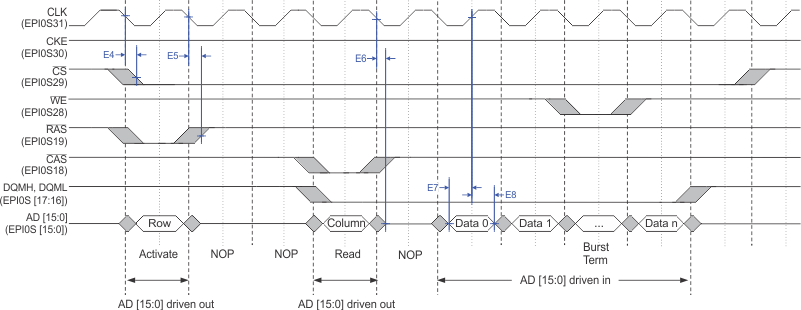 Figure 5-23 SDRAM Read Timing
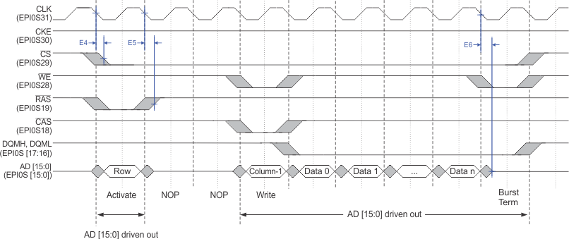 Figure 5-24 SDRAM Write Timing
Table 5-53 EPI Host-Bus 8 and Host-Bus 16 Interface Switching Characteristics Over Recommended Operating Conditions (Unless Otherwise Noted)
(see Figure 5-25, Figure 5-26, Figure 5-27, and Figure 5-28)
| NO. | PARAMETER | MIN | TYP | MAX | UNIT | |
|---|---|---|---|---|---|---|
| E16 | td(WR-WDATAV) | Delay time, WR to write data valid | 5 | ns | ||
| E17 | td(WRIV-DATA) | Delay time, WR invalid to data | 2 | EPI clocks | ||
| E18 | td(CS-OV) | Delay time, CS to output valid | –5 | 5 | ns | |
| E19 | td(CS-OIV) | Delay time, CS to output invalid | –5 | 5 | ns | |
| E20 | tw(STL) | Pulse duration, WR/RD strobe low | 2 | EPI clocks | ||
| E22 | tw(ALEH) | Pulse duration, ALE high | 1 | EPI clocks | ||
| E23 | tw(CSL) | Pulse duration, CS low | 4 | EPI clocks | ||
| E24 | td(ALE-ST) | Delay time, ALE rising to WR/RD strobe falling | 2 | EPI clocks | ||
| E25 | td(ALE-ADHZ) | Delay time, ALE falling to Address/Data high-impedance | 1 | EPI clocks | ||
Table 5-54 EPI Host-Bus 8 and Host-Bus 16 Interface Timing Requirements(1)
(see Figure 5-25 and Figure 5-27)
| NO. | MIN | MAX | UNIT | ||
|---|---|---|---|---|---|
| E14 | tsu(RDATA) | Setup time, read data | 10 | ns | |
| E15 | th(RDATA) | Hold time, read data | 0 | ns | |
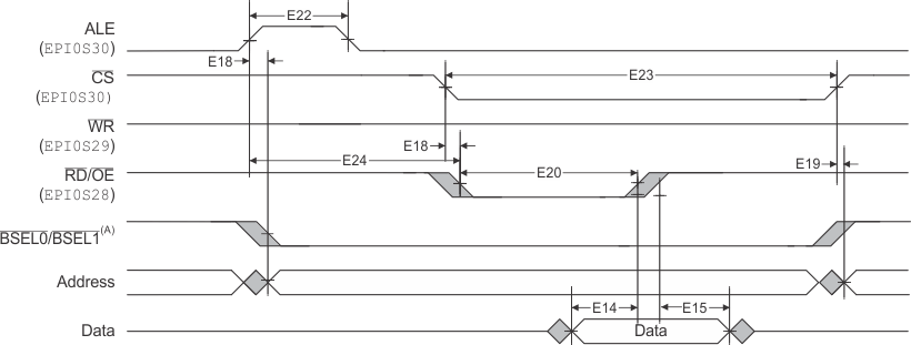
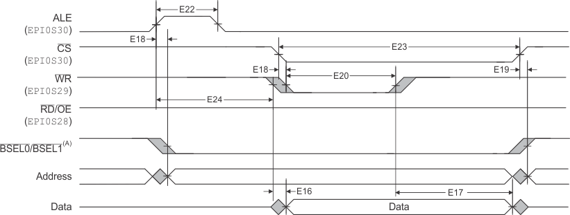


Table 5-55 EPI General-Purpose Interface Switching Characteristics Over Recommended Operating Conditions (Unless Otherwise Noted) (see Figure 5-29)
| NO. | PARAMETER | MIN | MAX | UNIT | |
|---|---|---|---|---|---|
| E26 | tw(CKH) | Pulse duration, general-purpose clock high | 10 | ns | |
| E27 | tw(CKL) | Pulse duration, general-purpose clock low | 10 | ns | |
| E30 | td(CK-OV) | Delay time, falling clock edge to output valid | –5 | 5 | ns |
| E31 | td(CK-OIV) | Delay time, falling clock edge to output invalid | –5 | 5 | ns |
| E33 | tc(CK) | Cycle time, general-purpose clock | 20 | ns | |
Table 5-56 EPI General-Purpose Interface Timing Requirements (see Figure 5-29 and Figure 5-30)
| NO. | MIN | MAX | UNIT | ||
|---|---|---|---|---|---|
| E28 | tsu(IN-CK) | Setup time, input signal before rising clock edge | 10 | ns | |
| E29 | th(CK-IN) | Hold time, input signal after rising clock edge | 0 | ns | |
| E32 | tsu(IRDY-CK) | Setup time, iRDY assertion or deassertion before falling clock edge | 10 | ns | |
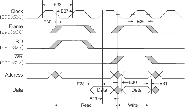
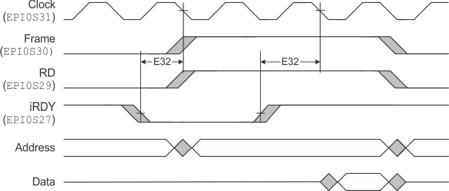 Figure 5-30 General-Purpose Mode iRDY Timing
5.11 Master Subsystem Peripherals
Master Subsystem peripherals are located on the APB Bus and AHB Bus, and are accessible from the Cortex-M3 CPU/µDMA. The AHB peripherals include EPI, USB, and two CAN modules. The APB peripherals include EMAC, two I2Cs, five UARTs, four SSIs, four GPTIMERs, two WDOGs, NMI WDOG, and a µCRC module (Cyclic Redundancy Check). The Cortex-M3 CPU/µDMA also have access to Analog (Result Registers only) and Shared peripherals (see Section 5.10).
For detailed information on the processor peripherals, see the Concerto F28M36x Technical Reference Manual (SPRUHE8).
5.11.1 Synchronous Serial Interface
This device has four SSI modules. Each SSI has a Master or Slave interface for synchronous serial communication with peripheral devices that have Texas Instruments™ SSIs, SPI, or Freescale™ serial format.
The SSI peripheral performs serial-to-parallel conversion on data received from a peripheral device. The CPU accesses data, control, and status information. The transmit and receive paths are buffered with internal FIFO memories, allowing up to eight 16-bit values to be stored independently in both transmit and receive modes. The SSI also supports µDMA transfers. The transmit and receive FIFOs can be programmed as destination/source addresses in the µDMA module. An µDMA operation is enabled by setting the appropriate bit or bits in the SSIDMACTL register.
Figure 5-31 shows the SSI peripheral.
5.11.1.1 Bit Rate Generation
The SSI includes a programmable bit-rate clock divider and prescaler to generate the serial output clock. Bit rates are supported to 2 MHz and higher, although maximum bit rate is determined by peripheral devices. The serial bit rate is derived by dividing-down the input clock (SysClk). The clock is first divided by an even prescale value CPSDVSR from 2 to 254, which is programmed in the SSI Clock Prescale (SSICPSR) register. The clock is further divided by a value from 1 to 256, which is 1 + SCR, where SCR is the value programmed in the SSI Control 0 (SSICR0) register. The frequency of the output clock SSIClk is defined by:
NOTE
For master mode, the system clock must be at least four times faster than SSIClk, with the restriction that SSIClk cannot be faster than 25 MHz. For slave mode, the system clock must be at least 12 times faster than SSIClk.
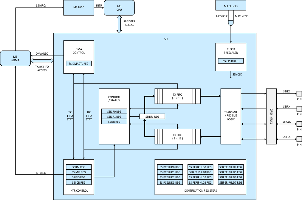 Figure 5-31 SSI
5.11.1.2 Transmit FIFO
The transmit FIFO is a 16-bit-wide, 8-location-deep, first-in, first-out memory buffer. The CPU writes data to the FIFO through the SSI Data (SSIDR) register, and data is stored in the FIFO until the data is read out by the transmission logic. When configured as a master or a slave, parallel data is written into the transmit FIFO before serial conversion and transmission to the attached slave or master, respectively, through the SSITx pin.
In slave mode, the SSI transmits data each time the master initiates a transaction. If the transmit FIFO is empty and the master initiates a transaction, the slave transmits the 8th most recent value in the transmit FIFO. If less than eight values have been written to the transmit FIFO since the SSI module clock was enabled using the SSI bit in the RGCG1 register, then "0" is transmitted. Care should be taken to ensure that valid data is in the FIFO as needed. The SSI can be configured to generate an interrupt or an µDMA request when the FIFO is empty.
5.11.1.3 Receive FIFO
The receive FIFO is a 16-bit-wide, 8-location-deep, first-in, first-out memory buffer. Received data from the serial interface is stored in the buffer until read out by the CPU, which accesses the read FIFO by reading the SSIDR register. When configured as a master or slave, serial data received through the SSIRx pin is registered before parallel loading into the attached slave or master receive FIFO, respectively.
5.11.1.4 Interrupts
The SSI can generate interrupts when the following conditions are observed:
- Transmit FIFO service (when the transmit FIFO is half full or less)
- Receive FIFO service (when the receive FIFO is half full or more)
- Receive FIFO time-out
- Receive FIFO overrun
- End of transmission
All of the interrupt events are ORed together before being sent to the interrupt controller, so the SSI generates a single interrupt request to the controller regardless of the number of active interrupts. Each of the four individual maskable interrupts can be masked by clearing the appropriate bit in the SSI Interrupt Mask (SSIIM) register. Setting the appropriate mask bit enables the interrupt.
The individual outputs, along with a combined interrupt output, allow the use of either a global interrupt service routine or modular device drivers to handle interrupts. The transmit and receive dynamic data-flow interrupts have been separated from the status interrupts so that data can be read or written in response to the FIFO trigger levels. The status of the individual interrupt sources can be read from the SSI Raw Interrupt Status (SSIRIS) and SSI Masked Interrupt Status (SSIMIS) registers.
The receive FIFO has a time-out period that is 32 periods at the rate of SSIClk (whether or not SSIClk is currently active) and is started when the RX FIFO goes from EMPTY to not-EMPTY. If the RX FIFO is emptied before 32 clocks have passed, the time-out period is reset. As a result, the ISR should clear the Receive FIFO Time-out Interrupt just after reading out the RX FIFO by writing a "1" to the RTIC bit in the SSI Interrupt Clear (SSIICR) register. The interrupt should not be cleared so late that the ISR returns before the interrupt is actually cleared, or the ISR may be reactivated unnecessarily.
The End-of-Transmission (EOT) interrupt indicates that the data has been transmitted completely. This interrupt can be used to indicate when it is safe to turn off the SSI module clock or enter sleep mode. In addition, because transmitted data and received data complete at exactly the same time, the interrupt can also indicate that read data is ready immediately, without waiting for the receive FIFO time-out period to complete.
5.11.1.5 Frame Formats
Each data frame is between 4 bits and 16 bits long, depending on the size of data programmed, and is transmitted starting with the MSB. The following basic frame types can be selected:
- Texas Instruments Synchronous Serial
- Freescale SPI
For all three formats, the serial clock (SSIClk) is held inactive while the SSI is idle, and SSIClk transitions at the programmed frequency only during active transmission or reception of data. The idle state of SSIClk is used to provide a receive time-out indication that occurs when the receive FIFO still contains data after a time-out period.
5.11.2 Universal Asynchronous Receiver/Transmitter
This device has five UART modules. The CPU accesses data, control, and status information. The UART also supports µDMA transfers. Each UART performs functions of parallel-to-serial and serial-to-parallel conversions. Each of the five UART modules is similar in functionality to a 16C550 UART, but is not register-compatible.
The UART is configured for transmit and receive via the TXE bit and the RXE bit, respectively, of the UART Control (UARTCTL) register. Transmit and receive are both enabled out of reset. Before any control registers are programmed, the UART must be disabled by clearing the UARTEN bit in UARTCTL. If the UART is disabled during a TX or RX operation, the current transaction is completed before the UART stops.
The UART module also includes a serial IR (SIR) encoder/decoder block that can be connected to an infrared transceiver to implement an IrDA SIR physical layer. The SIR function is programmed using the UARTCTL register.
Figure 5-32 shows the UART peripheral.
5.11.2.1 Baud-Rate Generation
The baud-rate divisor is a 22-bit number consisting of a 16-bit integer and a 6-bit fractional part. The number formed by these two values is used by the baud-rate generator to determine the bit period. Having a fractional baud-rate divider allows the UART to generate all the standard baud rates.
The 16-bit integer is loaded through the UART Integer Baud-Rate Divisor (UARTIBRD) register, and the 6-bit fractional part is loaded with the UART Fractional Baud-Rate Divisor (UARTFBRD) register. The baud rate divisor (BRD) has the following relationship to the system clock (where BRDI is the integer part of the BRD, and BRDF is the fractional part, separated by a decimal place).
where UARTSysClk is the system clock connected to the UART, and ClkDiv is either 16 (if HSE in UARTCTL is clear) or 8 (if HSE is set).
The 6-bit fractional number (that is to be loaded into the DIVFRAC bit field in the UARTFBRD register) can be calculated by taking the fractional part of the baud-rate divisor, multiplying this fractional part by 64, and adding 0.5 to account for rounding errors:
The UART generates an internal baud-rate reference clock at 8x or 16x the baud rate [referred to as Baud8 and Baud16, depending on the setting of the HSE bit (bit 5 in UARTCTL)]. This reference clock is divided by 8 or 16 to generate the transmit clock, and is used for error detection during receive operations.
Along with the UART Line Control, High Byte (UARTLCRH) register, the UARTIBRD and UARTFBRD registers form an internal 30-bit register. This internal register is only updated when a write operation to UARTLCRH is performed, so any changes to the baud-rate divisor must be followed by a write to the UARTLCRH register for the changes to take effect.
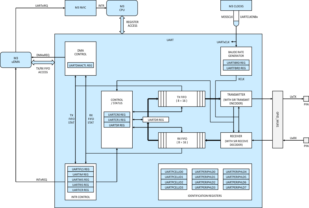 Figure 5-32 UART
5.11.2.2 Transmit and Receive Logic
The transmit logic performs parallel-to-serial conversion on the data read from the transmit FIFO. The control logic outputs the serial bit stream beginning with a start bit and followed by the data bits (LSB first), parity bit, and the stop bits according to the programmed configuration in the control registers.
The receive logic performs serial-to-parallel conversion on the received bit stream after a valid start pulse has been detected. Overrun, parity, frame error checking, and line-break detection are also performed, and their status accompanies the data that is written to the receive FIFO.
5.11.2.3 Data Transmission and Reception
Data received or transmitted is stored in two 16-byte FIFOs, though the receive FIFO has an extra 4 bits per character for status information. For transmission, data is written into the transmit FIFO. If the UART is enabled, a data frame starts transmitting with the parameters indicated in the UARTLCRH register. Data continues to be transmitted until there is no data left in the transmit FIFO. The BUSY bit in the UART Flag (UARTFR) register is asserted as soon as data is written to the transmit FIFO (that is, if the FIFO is nonempty) and remains asserted while data is being transmitted. The BUSY bit is negated only when the transmit FIFO is empty, and the last character has been transmitted from the shift register, including the stop bits. The UART can indicate that it is busy even though the UART may no longer be enabled.
When the receiver is idle (the UnRx signal is continuously "1"), and the data input goes Low (a start bit has been received), the receive counter begins running and data is sampled on the eighth cycle of Baud16 or the fourth cycle of Baud8, depending on the setting of the HSE bit (bit 5 in UARTCTL).
The start bit is valid and recognized if the UnRx signal is still low on the eighth cycle of Baud16 (HSE clear) or the fourth cycle of Baud 8 (HSE set), otherwise the start bit is ignored. After a valid start bit is detected, successive data bits are sampled on every 16th cycle of Baud16 or 8th cycle of Baud8 (that is, 1 bit period later), according to the programmed length of the data characters and value of the HSE bit in UARTCTL. The parity bit is then checked if parity mode is enabled. Data length and parity are defined in the UARTLCRH register.
Lastly, a valid stop bit is confirmed if the UnRx signal is High, otherwise a framing error has occurred. When a full word is received, the data is stored in the receive FIFO along with any error bits associated with that word.
5.11.2.4 Interrupts
The UART can generate interrupts when the following conditions are observed:
- Overrun Error
- Break Error
- Parity Error
- Framing Error
- Receive Time-out
- Transmit (when the condition defined in the TXIFLSEL bit in the UARTIFLS register is met, or if the EOT bit in UARTCTL is set, when the last bit of all transmitted data leaves the serializer)
- Receive (when the condition defined in the RXIFLSEL bit in the UARTIFLS register is met)
All of the interrupt events are ORed together before being sent to the interrupt controller, so the UART can only generate a single interrupt request to the controller at any given time. Software can service multiple interrupt events in a single interrupt service routine by reading the UART Masked Interrupt Status (UARTMIS) register.
The interrupt events that can trigger a controller-level interrupt are defined in the UART Interrupt Mask (UARTIM) register by setting the corresponding IM bits. If interrupts are not used, the raw interrupt status is always visible via the UART Raw Interrupt Status (UARTRIS) register.
Interrupts are always cleared (for both the UARTMIS and UARTRIS registers) by writing a "1" to the corresponding bit in the UART Interrupt Clear (UARTICR) register.
The receive time-out interrupt is asserted when the receive FIFO is not empty, and no further data is received over a 32-bit period. The receive time-out interrupt is cleared either when the FIFO becomes empty through reading all the data (or by reading the holding register), or when a "1" is written to the corresponding bit in the UARTICR register.
5.11.3 Cortex-M3 Inter-Integrated Circuit
This device has two Cortex-M3 I2C peripherals. The Cortex-M3 I2C bus provides bidirectional data transfer through a two-wire design (a serial data line SDA and a serial clock line SCL), and interfaces to external I2C devices such as serial memory (RAMs and ROMs), networking devices, LCDs, tone generators, and so on. The I2C bus may also be used for system testing and diagnostic purposes in product development and manufacture. The microcontroller includes two I2C modules, providing the ability to interact (both transmit and receive) with other I2C devices on the bus.
The two Cortex-M3 I2C modules include the following features:
- Devices on the I2C bus can be designated as either a master or a slave
- Supports both transmitting and receiving data as either a master or a slave
- Supports simultaneous master and slave operation
- Four I2C modes
- Master transmit
- Master receive
- Slave transmit
- Slave receive
- Two transmission speeds: Standard (100 Kbps) and Fast (400 Kbps)
- Master and slave interrupt generation
- Master generates interrupts when a transmit or receive operation completes (or aborts due to an error)
- Slave generates interrupts when data has been transferred or requested by a master or when a START or STOP condition is detected
- Master with arbitration and clock synchronization, multimaster support, and 7-bit addressing mode
Figure 5-33 shows the Cortex-M3 I2C peripheral.
5.11.3.1 Functional Overview
Each I2C module comprises both master and slave functions. For proper operation, the SDA and SCL pins must be configured as open-drain signals.
The I2C bus uses only two signals: SDA and SCL, named I2CSDA and I2CSCL. SDA is the bidirectional serial data line and SCL is the bidirectional serial clock line. The bus is considered idle when both lines are high.
Every transaction on the I2C bus is 9 bits long, consisting of eight data bits and a single acknowledge bit. The number of bytes per transfer (defined as the time between a valid START and STOP condition) is unrestricted, but each byte has to be followed by an acknowledge bit, and data must be transferred MSB first. When a receiver cannot receive another complete byte, the receiver can hold the clock line SCL Low and force the transmitter into a wait state. The data transfer continues when the receiver releases the clock SCL.
5.11.3.2 Available Speed Modes
The I2C bus can run in either standard mode (100 Kbps) or fast mode (400 Kbps). The selected mode should match the speed of the other I2C devices on the bus.
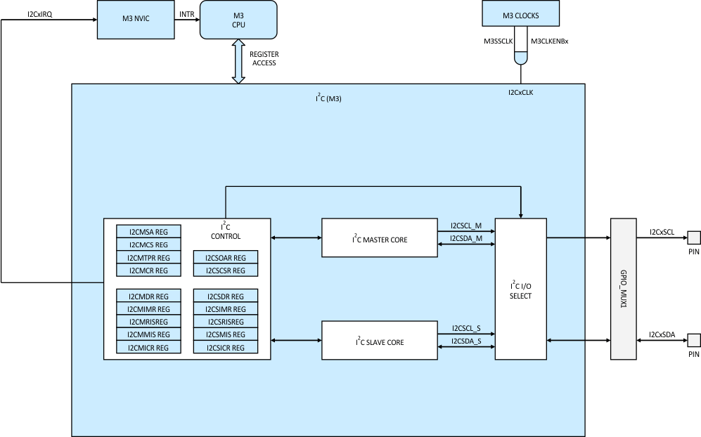 Figure 5-33 I2C (Cortex-M3)
5.11.3.3 I2C Electrical Data and Timing
Table 5-57 I2C Timing
| TEST CONDITIONS | MIN | MAX | UNIT | ||
|---|---|---|---|---|---|
| fSCL | SCL clock frequency | I2C clock module frequency is between 7 MHz and 12 MHz and I2C prescaler and clock divider registers are configured appropriately | 400 | kHz | |
| vil | Low level input voltage | 0.3 VDDIO | V | ||
| Vih | High level input voltage | 0.7 VDDIO | V | ||
| Vhys | Input hysteresis | 0.05 VDDIO | V | ||
| Vol | Low level output voltage | 3 mA sink current | 0 | 0.4 | V |
| tLOW | Low period of SCL clock | I2C clock module frequency is between 7 MHz and 12 MHz and I2C prescaler and clock divider registers are configured appropriately | 1.3 | μs | |
| tHIGH | High period of SCL clock | I2C clock module frequency is between 7 MHz and 12 MHz and I2C prescaler and clock divider registers are configured appropriately | 0.6 | μs | |
| lI | Input current with an input voltage between 0.1 VDDIO and 0.9 VDDIO MAX | –10 | 10 | μA | |
5.11.4 Cortex-M3 Controller Area Network
NOTE
The CAN module uses the popular IP known as D_CAN. This document uses the names “CAN” and “D_CAN” interchangeably to reference this peripheral.
This device has two Cortex-M3 CAN peripherals. CAN is a serial communications protocol that efficiently supports distributed real-time control with a high level of security. The CAN module supports bit rates up to 1 Mbit/s and is compliant with the ISO11898-1 (CAN 2.0B) protocol specification.
CAN implements the following features:
- CAN protocol version 2.0 part A, B
- Bit rates up to 1 Mbit/s
- Multiple clock sources
- 32 message objects
- Individual identifier mask for each message object
- Programmable FIFO mode for message objects
- Programmable loop-back modes for self-test operation
- Suspend mode for debug support
- Software module reset
- Automatic bus on after Bus-Off state by a programmable 32-bit timer
- Message RAM parity check mechanism
- Two interrupt lines
- Global power down and wakeup support
Figure 5-34 shows the Cortex-M3 CAN peripheral.
5.11.4.1 Functional Overview
CAN performs CAN protocol communication according to ISO 11898-1 (identical to Bosch® CAN protocol specification 2.0 A, B). The bit rate can be programmed to values up to 1 Mbit/s. Additional transceiver hardware is required for the connection to the physical layer (CAN bus).
For communication on a CAN network, individual message objects can be configured. The message objects and identifier masks are stored in the Message RAM. All functions concerning the handling of messages are implemented in the message handler. Those functions are: acceptance filtering, the transfer of messages between the CAN Core and the Message RAM, and the handling of transmission requests.
The register set of the CAN is accessible directly by the CPU via the module interface. These registers are used to control/configure the CAN Core and the message handler, and to access the message RAM.
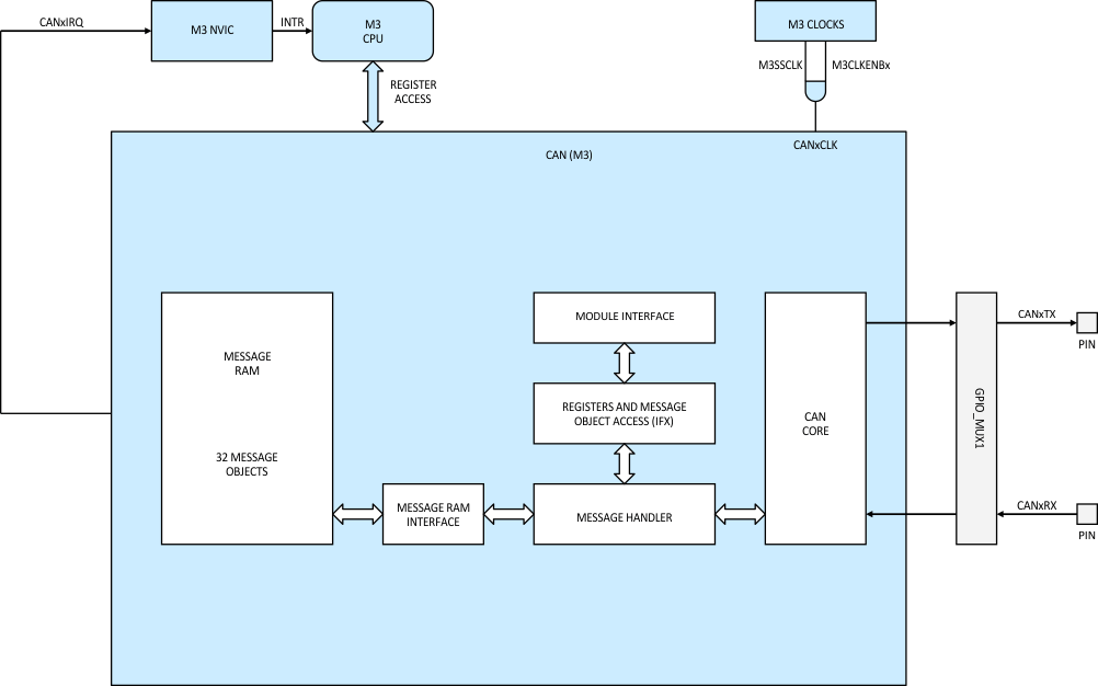 Figure 5-34 CAN (Cortex-M3)
5.11.5 Cortex-M3 Universal Serial Bus Controller
This device has one Cortex-M3 USB controller. The USB controller operates as a full-speed or low-speed function controller during point-to-point communications with the USB Host, Device, or OTG functions. The controller complies with the USB 2.0 standard, which includes SUSPEND and RESUME signaling. Thirty-two endpoints, which comprised of 2 hardwired endpoints for control transfers (one endpoint for IN and one endpoint for OUT) and 30 endpoints defined by firmware, along with a dynamic sizable FIFO, support multiple packet queuing. DMA access to the FIFO allows minimal interference from system software. Software-controlled connect and disconnect allow flexibility during USB device start-up. The controller complies with the OTG standard's Session Request Protocol (SRP) and Host Negotiation Protocol (HNP).
The USB controller includes the following features:
- Complies with USB-IF certification standards
- USB 2.0 full-speed (12-Mbps) and low-speed (1.5-Mbps) operation
- Integrated PHY
- Four transfer types: Control, Interrupt, Bulk, and Isochronous
- 32 endpoints:
- One dedicated control IN endpoint and one dedicated control OUT endpoint
- 15 configurable IN endpoints and 15 configurable OUT endpoints
- 4KB dedicated endpoint memory: one endpoint may be defined for double-buffered 1023-byte isochronous packet size
- VBUS droop and valid ID detection and interrupt
- Efficient transfers using DMA controller:
- Separate channels for transmit and receive for up to three IN endpoints and three OUT endpoints
- Channel requests asserted when FIFO contains required amount of data
- Electrical specifications are compliant with the USB Specification Rev. 2.0 (full-speed and low-speed support) and the On-The-Go Supplement to the USB 2.0 Specification Rev. 1.0. Some components of the USB system are integrated within the Concerto microcontroller and are specific to its design.
Figure 5-35 shows the USB peripheral.
5.11.5.1 Functional Description
The USB controller provides full OTG negotiation by supporting both the SRP and the HNP. The SRP allows devices on the B side of a cable to request the A-side devices' turn on VBUS. The HNP is used after the initial session request protocol has powered the bus and provides a method to determine which end of the cable will act as the Host controller. When the device is connected to non-OTG peripherals or devices, the controller can detect which cable end was used and provides a register to indicate if the controller should act as the Host controller or the Device controller. This indication and the mode of operation are handled automatically by the USB controller. This autodetection allows the system to use a single A/B connector instead of having both A and B connectors in the system, and supports full OTG negotiations with other OTG devices.
In addition, the USB controller provides support for connecting to non-OTG peripherals or Host controllers. The USB controller can be configured to act as either a dedicated Host or Device, in which case, the USB0VBUS and USB0ID signals can be used as GPIOs. However, when the USB controller is acting as a self-powered Device, a GPIO input must be connected to VBUS and configured to generate an interrupt when the VBUS level drops. This interrupt is used to disable the pullup resistor on the USB0DP signal.
NOTE
When the USB is used, the system clock frequency (SYSCLK) must be at least 20 MHz.
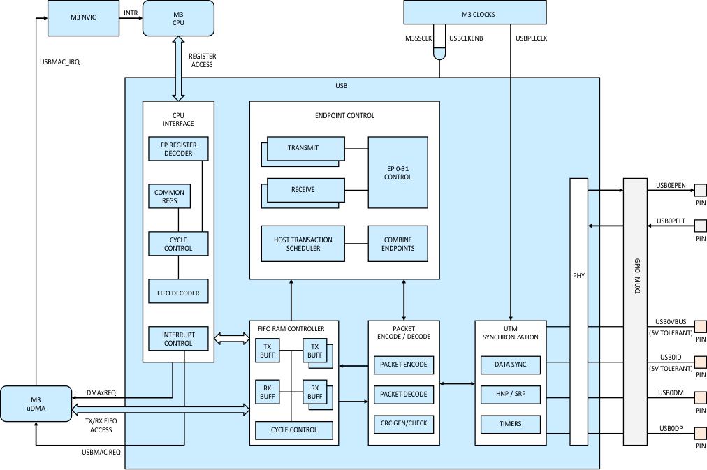 Figure 5-35 USB
5.11.6 Cortex-M3 Ethernet Media Access Controller
The Cortex-M3 EMAC conforms to IEEE 802.3 specifications and fully supports 10BASE-T and 100BASE-TX standards. This device has one Ethernet Media Access Controller.
The EMAC module has the following features:
- Conforms to the IEEE 802.3-2002 specification
- 10BASE-T/100BASE-TX IEEE-802.3 compliant
- Multiple operational modes
- Full- and half-duplex 100-Mbps
- Full- and half-duplex 10-Mbps
- Power-saving and power-down modes
- Highly configurable:
- Programmable MAC address
- Promiscuous mode support
- CRC error-rejection control
- User-configurable interrupts
- IEEE 1588 Precision Time Protocol: Provides highly accurate time stamps for individual packets
- Efficient transfers using the Micro Direct Memory Access Controller (µDMA)
- Separate channels for transmit and receive
- Receive channel request asserted on packet receipt
- Transmit channel request asserted on empty transmit FIFO
Figure 5-36 shows the EMAC peripheral.
5.11.6.1 Functional Overview
The Ethernet Controller is functionally divided into two layers: the Media Access Controller (MAC) layer and the Network Physical (PHY) layer. The MAC resides inside the device, and the PHY outside of the device. These layers correspond to the OSI model layers 2 and 1, respectively. The CPU accesses the Ethernet Controller via the MAC layer. The MAC layer provides transmit and receive processing for Ethernet frames. The MAC layer also provides the interface to the external PHY layer via an internal Media Independent Interface (MII). The PHY layer communicates with the Ethernet bus.
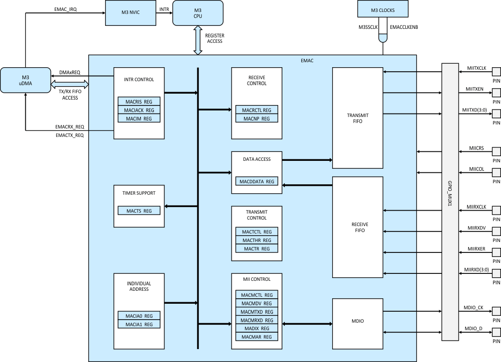 Figure 5-36 EMAC
5.11.6.2 MII Signals
The individual EMAC and Management Data Input/Output (MDIO) signals for the MII interface are summarized in Table 5-58.
Table 5-58 EMAC and MDIO Signals for MII Interface
| SIGNAL | TYPE(1) | DESCRIPTION |
|---|---|---|
| MIITXCK | I | Transmit clock. The transmit clock is a continuous clock that provides the timing reference for transmit operations. The MIITXD and MIITXEN signals are tied to this clock. The clock is generated by the PHY and is 2.5 MHz at 10-Mbps operation and 25 MHz at 100-Mbps operation. |
| MIITXER | O | This pin is always driven low from the MAC controller on the device. |
| MIITXD[3-0] | O | Transmit data. The transmit data pins are a collection of four data signals comprising 4 bits of data. MTDX0 is the least-significant bit (LSB). The signals are synchronized by MIITXCLK and are valid only when MIITXEN is asserted. |
| MIITXEN | O | Transmit enable. The transmit enable signal indicates that the MIITXD pins are generating nibble data for use by the PHY. MIITXEN is driven synchronously to MIITXCLK. |
| MIICOL | I | Collision detected. In half-duplex operation, the MIICOL pin is asserted by the PHY when the PHY detects a collision on the network. The MIICOL pin remains asserted while the collision condition persists. This signal is not necessarily synchronous to MIITXCLK or MIIRXCLK. In full-duplex operation, the MIICOL pin is used for hardware transmit flow control. Asserting the MIICOL pin will stop packet transmissions; packets in the process of being transmitted when MIICOL is asserted will complete transmission. The MIICOL pin should be held low if hardware transmit flow control is not used. |
| MIICRS | I | Carrier sense. In half-duplex operation, the MIICRS pin is asserted by the PHY when the network is not idle in either transmit or receive. The pin is deasserted when both transmit and receive are idle. This signal is not necessarily synchronous to MIITXCLK or MIIRXCLK. In full-duplex operation, the MIICRS pin should be held low. |
| MIIRXCK | I | Receive clock. The receive clock is a continuous clock that provides the timing reference for receive operations. The MIIRXD, MIIRXDV, and MIIRXER signals are tied to this clock. The clock is generated by the PHY and is 2.5 MHz at 10-Mbps operation and 25 MHz at 100-Mbps operation. |
| MIIRXD[3-0] | I | Receive data. The receive data pins are a collection of four data signals comprising 4 bits of data. MRDX0 is the least-significant bit. The signals are synchronized by MIIRXCLK and are valid only when MIIRXDV is asserted. |
| MIIRXDV | I | Receive data valid. The receive data valid signal indicates that the MIIRXD pins are generating nibble data for use by the EMAC. MIIRXDV is driven synchronously to MIIRXCLK. |
| MIIRXER | I | Receive error. The receive error signal is asserted for one or more MIIRXCLK periods to indicate that an error was detected in the received frame. The MIIRXER signal being asserted is meaningful only during data reception when MIIRXDV is active. |
| MDIO_CK | O | Management data clock. The MDIO data clock is sourced by the MDIO module on the system. MDIO_CK is used to synchronize MDIO data access operations done on the MDIO pin. The frequency of this clock is controlled by the CLKDIV bits in the MDIO Control Register (CONTROL). |
| MDIO_D | I/O | Management data input output. The MDIO data pin drives PHY management data into and out of the PHY by way of an access frame that consists of start-of-frame, read/write indication, PHY address, register address, and data bit cycles. The MDIO_D pin acts as an output for all but the data bit cycles, at which time the pin is an input for read operations. |
5.11.6.3 EMAC Electrical Data and Timing
Table 5-59 Timing Requirements for MIITXCK (see Figure 5-37)
| NO. | 100 Mbps | 10 Mbps | UNIT | ||||
|---|---|---|---|---|---|---|---|
| MIN | MAX | MIN | MAX | ||||
| 1 | tc(TXCK) | Cycle time, MIITXCK (25 MHz) | 40 | 40 | ns | ||
| Cycle time, MIITXCK (2.5 MHz) | 400 | 400 | |||||
| 2 | tw(TXCKH) | Pulse duration, MIITXCK high | 16 | 24 | 196 | 204 | ns |
| 3 | tw(TXCKL) | Pulse duration, MIITXCK low | 16 | 24 | 196 | 204 | ns |
 Figure 5-37 100/10Mb/s MII Transmit Clock Timing
Table 5-60 Timing Requirements for MIIRXCK (see Figure 5-38)
| NO. | 100 Mbps | 10 Mbps | UNIT | ||||
|---|---|---|---|---|---|---|---|
| MIN | MAX | MIN | MAX | ||||
| 1 | tc(RXCK) | Cycle time, MIIRXCK (25 MHz) | 40 | 40 | ns | ||
| Cycle time, MIIRXCK (2.5 MHz) | 400 | 400 | |||||
| 2 | tw(RXCKH) | Pulse duration, MIIRXCK high | 16 | 24 | 196 | 204 | ns |
| 3 | tw(RXCKL) | Pulse duration, MIIRXCK low | 16 | 24 | 196 | 204 | ns |
 Figure 5-38 100/10Mb/s MII Receive Clock Timing
Table 5-61 Switching Characteristics Over Recommended Operating Conditions (Unless Otherwise Noted) for EMAC MII Transmit (see Figure 5-39)
| NO. | PARAMETER | MIN | MAX | UNIT | |
|---|---|---|---|---|---|
| 1 | td(TXCKH-MTXDV) | Delay time, MIITXCK high to transmit selected signals valid | 5 | 25 | ns |
 Figure 5-39 100/10Mb/s MII Transmit Timing
Table 5-62 Timing Requirements for EMAC MII Receive (see Figure 5-40)
| NO. | MIN | NOM | MAX | UNIT | ||
|---|---|---|---|---|---|---|
| 1 | tsu(MRXDV-RXCKH) | Setup time, receive selected signals valid before MIIRXCK high | 8 | ns | ||
| 2 | th(RXCKH-MRXDV) | Hold time, receive selected signals valid after MIIRXCK high | 7 | ns | ||
 Figure 5-40 100/10Mb/s MII Receive Timing
5.11.6.4 MDIO Electrical Data and Timing
Table 5-63 Switching Characteristics Over Recommended Operating Conditions (Unless Otherwise Noted) for MDIO_CK (see Figure 5-41)
| NO. | PARAMETER | MIN | MAX | UNIT | |
|---|---|---|---|---|---|
| 1 | tc(MCK) | Cycle time, MDIO_CK (2.5 MHz) | 400 | 400 | ns |
| 2 | tw(MCKH) | Pulse duration, MDIO_CK high | 196 | 204 | ns |
| 3 | tw(MCKL) | Pulse duration, MDIO_CK low | 196 | 204 | ns |
 Figure 5-41 MII Serial Management Timing
Table 5-64 Switching Characteristics Over Recommended Operating Conditions (Unless Otherwise Noted) for MDIO as Output (see Figure 5-42)
| NO. | PARAMETER | MIN | MAX | UNIT | |
|---|---|---|---|---|---|
| 1 | td(MCKH-MDV) | Delay time, MDIO_CK high to MDIO_D valid | 5 | 25 | ns |
 Figure 5-42 MII Serial Management Timing – MDIO as Output
Table 5-65 Timing Requirements for MDIO as Input (see Figure 5-43)
| NO. | MIN | NOM | MAX | UNIT | ||
|---|---|---|---|---|---|---|
| 4 | tsu(MDV-MCKH) | Setup time, MDIO_D valid before MDIO_CK high | 20 | ns | ||
| 5 | th(MCKH-MDV) | Hold time, MDIO_D valid after MDIO_CK high | 7 | ns | ||
 Figure 5-43 MII Serial Management Timing – MDIO as Input
5.12 Control Subsystem Peripherals
Control Subsystem peripherals are accessible from the C28x CPU via the C28x Memory Bus, and from the C28x DMA via the C28x DMA Bus. They include one NMI Watchdog, three Timers, four Serial Port Peripherals (SCI, SPI, McBSP, I2C), and three types of Control Peripherals (ePWM, eQEP, eCAP). Additionally, the C28x CPU/DMA also have access to the EPI, and to Analog and Shared peripherals (see Section 5.10).
For detailed information on the processor peripherals, see the Concerto F28M36x Technical Reference Manual (SPRUHE8).
5.12.1 High-Resolution PWM and Enhanced PWM Modules
There are 12 PWM modules in the Concerto device. Eight of these are of the HRPWM type with high-resolution control on both A and B signal outputs, and four are of the ePWM type. The HRPWM modules have all the features of the ePWM plus they offer significantly higher PWM resolution (time granularity on the order of 150 ps). Figure 5-44 shows the eight HRPWM modules (PWM 1–8) and four ePWM modules (PWM 9–PWM12).
The synchronization inputs to the PWM modules include the SYNCI signal from the GPTRIP1 output of GPIO_MUX1, and the TBCLKSYNC signal from the CPCLKCR0 register. Synchronization output SYNCO1 comes from the ePWM1 module and is stretched by 8 HSPCLK cycles before entering GPIO_MUX1. There are two groups of trip signal inputs to PWM modules. TRIP1–15 inputs come from GPTRIP1–12 (from GPIO_MUX1), ECCDBLERR signal (from C28x Local and Shared RAM), and PIEERR signal from the C28x CPU. TZ1–6 (Trip Zone) inputs come from GPTRIP 1–3 (from GPIO_MUX1), EQEPERR (from the eQEP peripheral), CLOCKFAIL (from M3 CLOCKS), and EMUSTOP (from the C28x CPU).
There are 12 SOCA PWM outputs and 12 SOCB PWM outputs—a pair from each PWM module. The 12 SOCA outputs are OR-ed together and stretched by 32 HSPCLK cycles before entering GPIO_MUX1 as a single SOCAO signal. The 12 SOCB outputs are OR-ed together and stretched by 32 HSPCLK cycles before entering GPIO_MUX1 as a single SOCBO signal. The 18 SOCA/B outputs from PWM1–PWM9 also go to the Analog Subsystem, where they can be selected to become conversion triggers to ADC modules.
The 12 PWM modules also drive two other sets of outputs which can interrupt the C28x CPU via the C28x PIE block. These are 12 EPWMINT interrupts and 12 EPWMTZINT trip-zone interrupts. See Figure 5-45 for the internal structure of the HRPWM and ePWM modules. The green-colored blocks are common to both ePWM and HRPWM modules, but only the HRPWMs have the grey-colored hi-resolution blocks.
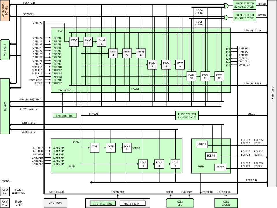 Figure 5-44 PWM, eCAP, eQEP
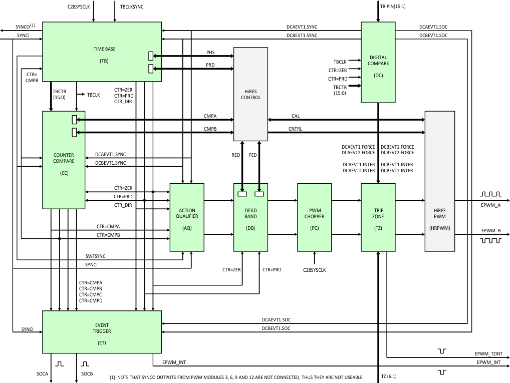 Figure 5-45 Internal Structure of PWM
5.12.1.1 HRPWM Electrical Data and Timing
Table 5-66 shows the high-resolution PWM switching characteristics.
Table 5-66 High-Resolution PWM Characteristics at SYSCLKOUT = (60–150 MHz)
| PARAMETER | MIN | TYP | MAX | UNIT | |
|---|---|---|---|---|---|
| Micro Edge Positioning (MEP) step size(1) | 150 | 310 | ps | ||
Applications that use the HRPWM feature should use MEP Scale Factor Optimizer (SFO) estimation software functions. See the TI software libraries for details of using SFO function in end applications. SFO functions help to estimate the number of MEP steps per SYSCLKOUT period dynamically while the HRPWM is in operation.
5.12.1.2 ePWM Electrical Data and Timing
Table 5-67 shows the PWM timing requirements and Table 5-68 shows the PWM switching characteristics.
Table 5-67 ePWM Timing Requirements(1)
| MIN | MAX | UNIT | |||
|---|---|---|---|---|---|
| tw(SYCIN) | Sync input pulse width | Asynchronous | 2tc(SCO) | cycles | |
| Synchronous | 2tc(SCO) | cycles | |||
| With input qualifier | 1tc(SCO) + tw(IQSW) | cycles | |||
Table 5-68 ePWM Switching Characteristics
over recommended operating conditions (unless otherwise noted)| PARAMETER | TEST CONDITIONS | MIN | MAX | UNIT | |
|---|---|---|---|---|---|
| tw(PWM) | Pulse duration, PWMx output high/low | 20 | ns | ||
| tw(SYNCOUT) | Sync output pulse width | 8tc(SCO) | cycles | ||
| td(PWM)tza | Delay time, trip input active to PWM forced high Delay time, trip input active to PWM forced low |
no pin load | 25 | ns | |
| td(TZ-PWM)HZ | Delay time, trip input active to PWM Hi-Z | 20 | ns | ||
5.12.1.2.1 Trip-Zone Input Timing
Table 5-69 Trip-Zone Input Timing Requirements(1)
| MIN | MAX | UNIT | |||
|---|---|---|---|---|---|
| tw(TZ) | Pulse duration, TZx input low | Asynchronous | 1tc(SCO) | cycles | |
| Synchronous | 2tc(SCO) | cycles | |||
| With input qualifier | 1tc(SCO) + tw(IQSW) | cycles | |||

5.12.2 Enhanced Capture Module
There are six identical eCAP modules in Concerto devices: eCAP1, 2, 3, 4, 5, and 6. Each eCAP module represents one complete capture channel. Its main function is to accurately capture the timings of external events. One can also use eCAP modules for PWM, when they are not being used for input captures. This secondary function is selected by flipping the CAP/APWM bit of the ECCTL2 Register. For PWM function, the counter operates in count-up mode, providing a time base for asymmetrical pulse width (PWM) waveforms. The CAP1 and CAP2 registers become the period and compare registers, respectively; while the CAP3 and CAP4 registers become the shadow registers of the main period and capture registers, respectively.
The left side of Figure 5-47 shows internal components associated with the capture block, and the right side depicts the PWM block. The two blocks share a set of four registers that are used in both Capture and PWM modes. Other components include the Counter block that uses the SYNCIN and SYNCOUT ports to synchronize with other modules; and the Interrupt Trigger and Flag Control block that sends Capture, PWM, and Counter events to the C28x PIE block via the ECAPxINT output. There are six ECAPxINT interrupts—one for each eCAP module.
The eCAP peripherals are clocked by C28SYSCLK, and its registers are accessible by the C28x CPU. This peripheral clock can be enabled or disabled by flipping a bit in one of the system control registers.
5.12.2.1 eCAP Electrical Data and Timing
Table 5-70 shows the eCAP timing requirement and Table 5-71 shows the eCAP switching characteristics.
Table 5-70 eCAP Timing Requirement(1)
| MIN | MAX | UNIT | |||
|---|---|---|---|---|---|
| tw(CAP) | Capture input pulse width | Asynchronous | 2tc(SCO) | cycles | |
| Synchronous | 2tc(SCO) | cycles | |||
| With input qualifier | 1tc(SCO) + tw(IQSW) | cycles | |||
Table 5-71 eCAP Switching Characteristics
over recommended operating conditions (unless otherwise noted)| PARAMETER | TEST CONDITIONS | MIN | MAX | UNIT | |
|---|---|---|---|---|---|
| tw(APWM) | Pulse duration, APWMx output high/low | 20 | ns | ||
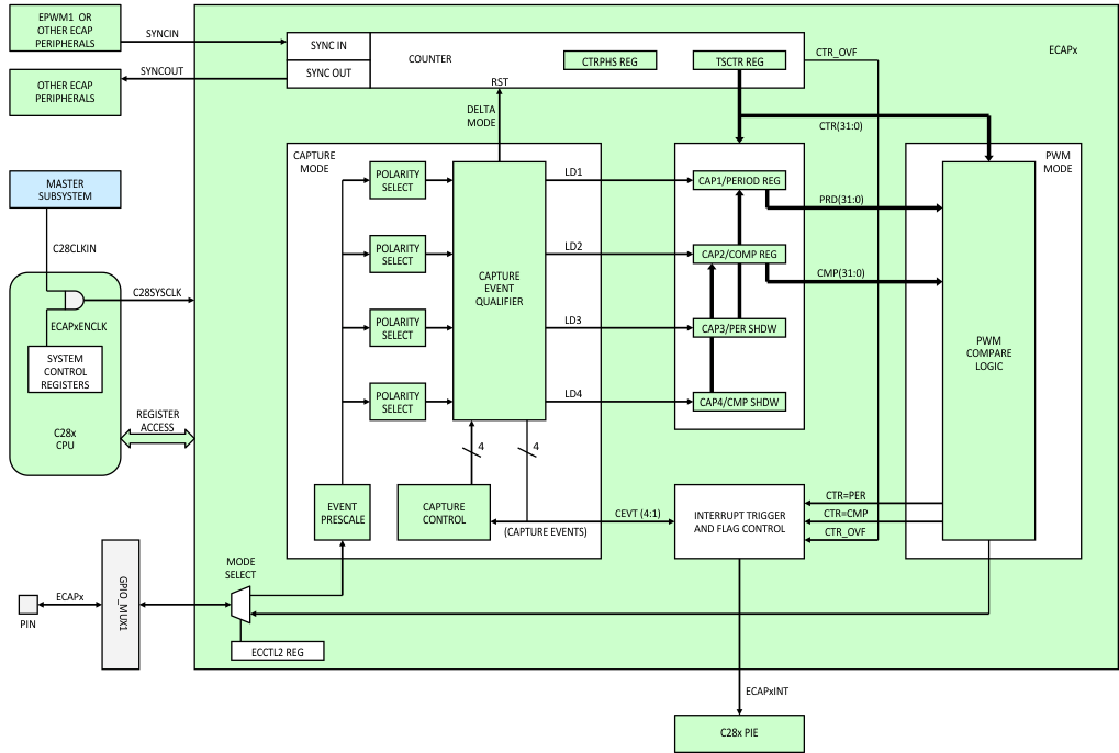 Figure 5-47 eCAP
5.12.3 Enhanced Quadrature Encoder Pulse Module
The eQEP module interfaces directly with linear or rotary incremental encoders to obtain position, direction, and speed information from rotating machines used in high-performance motion and position-control systems. There are three Type 0 eQEP modules in each Concerto device.
Each eQEP peripheral comprises five major functional blocks: Quadrature Capture Unit (QCAP), Position Counter/Control Unit (PCCU), Quadrature Decoder (QDU), Unit Time Base for speed and frequency measurement (UTIME), and Watchdog timer for detecting stalls (QWDOG). The C28x CPU controls and communicates with these modules through a set of associated registers (see Figure 5-48). The eQEP peripherals are clocked by C28SYSCLK, and its registers are accessible by the C28x CPU. This peripheral clock can be enabled or disabled by flipping a bit in one of the system control registers.
Each eQEP peripheral connects through the GPIO_MUX1 block to four device pins. Two of the four pins are always inputs, while the other two can be inputs or outputs, depending on the operating mode. The PCCU block of each eQEP also drives one interrupt to the C28x PIE. There is a total of three EQEPxINT interrupts—one from each of the three eQEP modules.
5.12.3.1 eQEP Electrical Data and Timing
Table 5-72 shows the eQEP timing requirement and Table 5-73 shows the eQEP switching characteristics.
Table 5-72 eQEP Timing Requirements(1)
| MIN | MAX | UNIT | |||
|---|---|---|---|---|---|
| tw(QEPP) | QEP input period | Asynchronous(2)/synchronous | 2tc(SCO) | cycles | |
| With input qualifier | 2[1tc(SCO) + tw(IQSW)] | cycles | |||
| tw(INDEXH) | QEP Index Input High time | Asynchronous(2)/synchronous | 2tc(SCO) | cycles | |
| With input qualifier | 2tc(SCO) + tw(IQSW) | cycles | |||
| tw(INDEXL) | QEP Index Input Low time | Asynchronous(2)/synchronous | 2tc(SCO) | cycles | |
| With input qualifier | 2tc(SCO) + tw(IQSW) | cycles | |||
| tw(STROBH) | QEP Strobe High time | Asynchronous(2)/synchronous | 2tc(SCO) | cycles | |
| With input qualifier | 2tc(SCO) + tw(IQSW) | cycles | |||
| tw(STROBL) | QEP Strobe Input Low time | Asynchronous(2)/synchronous | 2tc(SCO) | cycles | |
| With input qualifier | 2tc(SCO) + tw(IQSW) | cycles | |||
Table 5-73 eQEP Switching Characteristics
over recommended operating conditions (unless otherwise noted)| PARAMETER | TEST CONDITIONS | MIN | MAX | UNIT | |
|---|---|---|---|---|---|
| td(CNTR)xin | Delay time, external clock to counter increment | 4tc(SCO) | cycles | ||
| td(PCS-OUT)QEP | Delay time, QEP input edge to position compare sync output | 6tc(SCO) | cycles | ||
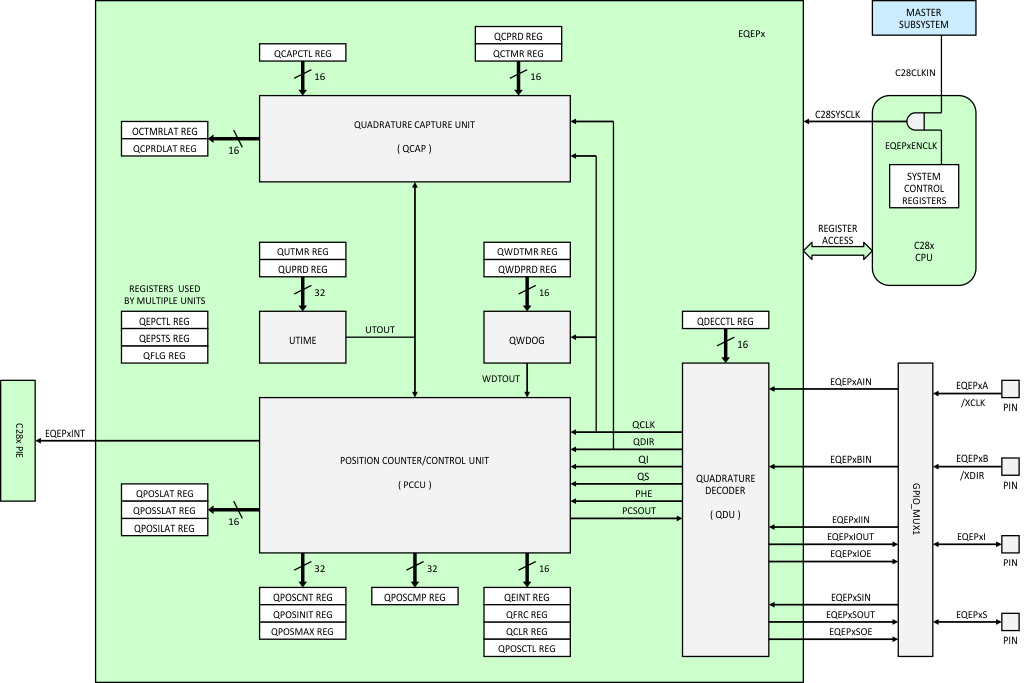 Figure 5-48 eQEP
5.12.4 C28x Inter-Integrated Circuit Module
This device has one C28x I2C peripheral. The I2C provides an interface between a Concerto device and devices compliant with the NXP® I2C-bus specification and user manual (UM10204) and connected by way of an I2C bus. External components attached to this 2-wire serial bus can transmit 1-bit to 8-bit data to and receive 1-bit to 8-bit data from the device through the I2C module.
NOTE
A unit of data transmitted or received by the I2C module can have fewer than 8 bits; however, for convenience, a unit of data is called a data byte in this section. The number of bits in a data byte is selectable via the BC bits of the mode register, I2CMDR.
The I2C module has the following features:
- Compliance with the NXP I2C-bus specification and user manual (UM10204):
- Support for 1-bit to 8-bit format transfers
- 7-bit and 10-bit addressing modes
- General call
- START byte mode
- Support for multiple master-transmitters and slave-receivers
- Support for multiple slave-transmitters and master-receivers
- Combined master transmit-and-receive and receive-and-transmit mode
- Data transfer rate of from 10 Kbps up to 400 Kbps (I2C Fast-mode rate)
- One 4-word receive FIFO and one 4-word transmit FIFO
- One interrupt that can be used by the CPU. This interrupt can be generated as a result of one of the following conditions:
- Transmit-data ready
- Receive-data ready
- Register-access ready
- No-acknowledgment received
- Arbitration lost
- Stop condition detected
- Addressed as slave
- An additional interrupt that can be used by the CPU when in FIFO mode
- Module enable or disable capability
- Free data format mode
The I2C module does not support:
- High-speed mode (Hs-mode)
- CBUS-compatibility mode
Figure 5-49 shows the C28x I2C peripheral.
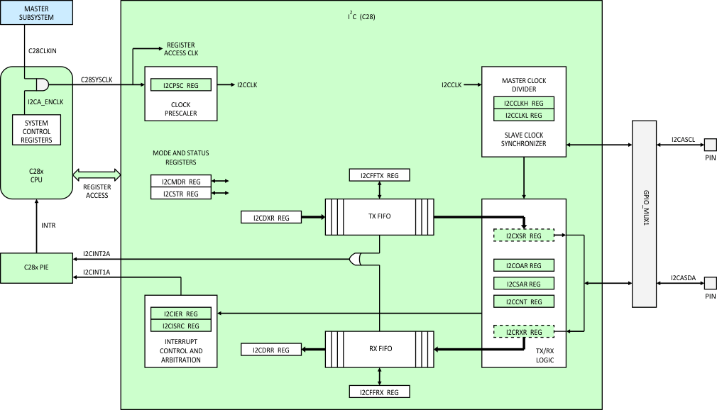 Figure 5-49 I2C (C28x)
5.12.4.1 Functional Overview
Each device connected to an I2C Bus is recognized by a unique address. Each device can operate as either a transmitter or a receiver, depending on the function of the device. A device connected to the I2C Bus can also be considered as the master or the slave when performing data transfers. A master device is the device that initiates a data transfer on the bus and generates the clock signals to permit that transfer. During this transfer, any device addressed by this master is considered a slave. The I2C module supports the multi-master mode, in which one or more devices capable of controlling an I2C Bus can be connected to the same I2C Bus.
For data communication, the I2C module has a serial data pin (SDA) and a serial clock pin (SCL). These two pins carry information between the C28x device and other devices connected to the I2C Bus. The SDA and SCL pins both are bidirectional. They each must be connected to a positive supply voltage using a pullup resistor. When the bus is free, both pins are high. The driver of these two pins has an open-drain configuration to perform the required wired-AND function. There are two major transfer techniques:
- Standard Mode: Send exactly n data values, where n is a value you program in an I2C module register.
- Repeat Mode: Keep sending data values until you use software to initiate a STOP condition or a new START condition.
The I2C module consists of the following primary blocks:
- A serial interface: one data pin (SDA) and one clock pin (SCL)
- Data registers and FIFOs to temporarily hold receive data and transmit data traveling between the SDA pin and the CPU
- Control and status registers
- A peripheral bus interface to enable the CPU to access the I2C module registers and FIFOs.
5.12.4.2 Clock Generation
The device clock generator receives a signal from an external clock source and produces an I2C input clock with a programmed frequency. The I2C input clock is equivalent to the CPU clock and is then divided twice more inside the I2C module to produce the module clock and the master clock.
5.12.4.3 I2C Electrical Data and Timing
Table 5-74 I2C Timing
| TEST CONDITIONS | MIN | MAX | UNIT | ||
|---|---|---|---|---|---|
| fSCL | SCL clock frequency | I2C clock module frequency is between 7 MHz and 12 MHz and I2C prescaler and clock divider registers are configured appropriately | 400 | kHz | |
| vil | Low level input voltage | 0.3 VDDIO | V | ||
| Vih | High level input voltage | 0.7 VDDIO | V | ||
| Vhys | Input hysteresis | 0.05 VDDIO | V | ||
| Vol | Low level output voltage | 3 mA sink current | 0 | 0.4 | V |
| tLOW | Low period of SCL clock | I2C clock module frequency is between 7 MHz and 12 MHz and I2C prescaler and clock divider registers are configured appropriately | 1.3 | μs | |
| tHIGH | High period of SCL clock | I2C clock module frequency is between 7 MHz and 12 MHz and I2C prescaler and clock divider registers are configured appropriately | 0.6 | μs | |
| lI | Input current with an input voltage between 0.1 VDDIO and 0.9 VDDIO MAX | –10 | 10 | μA | |
5.12.5 C28x Serial Communications Interface
This device has one SCI peripheral. SCI is a two-wire asynchronous serial port, commonly known as a UART. The SCI module supports digital communications between the CPU and other asynchronous peripherals that use the standard non-return-to-zero (NRZ) format
The SCI receiver and transmitter each have a 16-level-deep FIFO for reducing servicing overhead, and each has its own separate enable and interrupt bits. Both can be operated independently for half-duplex communication, or simultaneously for full-duplex communication. To specify data integrity, the SCI checks received data for break detection, parity, overrun, and framing errors. The bit rate is programmable to different speeds through a 16-bit baud-select register.
Features of the SCI module include:
- Two external pins:
- SCITXD: SCI transmit-output pin
- SCIRXD: SCI receive-input pin
- Baud rate programmable to 64K different rates
NOTE: Both pins can be used as GPIO if not used for SCI.
- Data-word format
- One start bit
- Data-word length programmable from 1 to 8 bits
- Optional even/odd/no parity bit
- One or two stop bits
- Four error-detection flags: parity, overrun, framing, and break detection
- Two wake-up multiprocessor modes: idle-line and address bit
- Half- or full-duplex operation
- Double-buffered receive and transmit functions
- Transmitter and receiver operations can be accomplished through interrupt-driven or polled algorithms with status flags.
- Transmitter: TXRDY flag (transmitter-buffer register is ready to receive another character) and TX EMPTY flag (transmitter-shift register is empty)
- Receiver: RXRDY flag (receiver-buffer register is ready to receive another character), BRKDT flag (break condition occurred), and RX ERROR flag (monitoring four interrupt conditions)
- Separate enable bits for transmitter and receiver interrupts (except BRKDT)
- NRZ format
NOTE
All registers in this module are 8-bit registers that are connected to Peripheral Frame 2. When a register is accessed, the register data is in the lower byte (bits 7–0), and the upper byte (bits 15–8) is read as zeros. Writing to the upper byte has no effect.
- Auto baud-detect hardware logic
- 16-level transmit and receive FIFO
Figure 5-50 shows the C28x SCI peripheral.
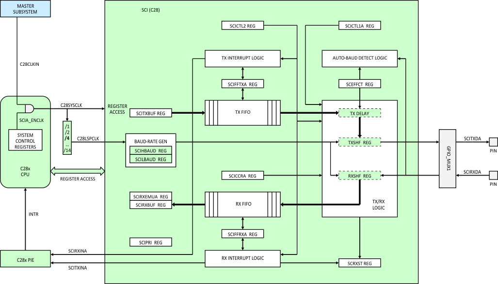 Figure 5-50 SCI (C28x)
5.12.5.1 Architecture
The major elements used in full-duplex operation include:
- A transmitter (TX) and its major registers:
- SCITXBUF register – Transmitter Data Buffer register. Contains data (loaded by the CPU) to be transmitted
- TXSHF register – Transmitter Shift register. Accepts data from the SCITXBUF register and shifts data onto the SCITXD pin, 1 bit at a time
- A receiver (RX) and its major registers:
- RXSHF register – Receiver Shift register. Shifts data in from the SCIRXD pin, 1 bit at a time
- SCIRXBUF register – Receiver Data Buffer register. Contains data to be read by the CPU. Data from a remote processor is loaded into the RXSHF register and then into the SCIRXBUF and SCIRXEMU registers
- A programmable baud generator
- Data-memory-mapped control and status registers enable the CPU to access the I2C module registers and FIFOs.
The SCI receiver and transmitter can operate either independently or simultaneously.
5.12.5.2 Multiprocessor and Asynchronous Communication Modes
The SCI has two multiprocessor protocols: the idle-line multiprocessor mode and the address-bit multiprocessor mode. These protocols allow efficient data transfer between multiple processors.
The SCI offers the UART communications mode for interfacing with many popular peripherals. The asynchronous mode requires two lines to interface with many standard devices such as terminals and printers that use RS-232-C formats.
Data transmission characteristics include:
- One start bit
- One to eight data bits
- An even/odd parity bit or no parity bit
- One or two stop bits with a programmed frequency
5.12.6 C28x Serial Peripheral Interface
This device has one C28x SPI. The SPI is a high-speed synchronous serial input/output (I/O) port that allows a serial bit stream of programmed length (1 to 16 bits) to be shifted into and out of the device at a programmed bit-transfer rate. The SPI is normally used for communications between the DSP controller and external peripherals or another controller. Typical applications include external I/O or peripheral expansion via devices such as shift registers, display drivers, and ADCs. Multi-device communications are supported by the master/slave operation of the SPI. The port supports a 16-level, receive-and-transmit FIFO for reducing CPU servicing overhead.
The SPI module features include:
- SPISOMI: SPI slave-output/master-input pin
- SPISIMO: SPI slave-input/master-output pin
- SPISTE: SPI slave transmit-enable pin
- SPICLK: SPI serial-clock pin
- Two operational modes: master and slave
- Baud rate: 125 different programmable rates. The maximum baud rate that can be employed is limited by the maximum speed of the I/O buffers used on the SPI pins.
- Data word length: 1 to 16 data bits
- Four clocking schemes (controlled by clock polarity and clock phase bits) include:
- Falling edge without phase delay: SPICLK active-high. SPI transmits data on the falling edge of the SPICLK signal and receives data on the rising edge of the SPICLK signal.
- Falling edge with phase delay: SPICLK active-high. SPI transmits data one half-cycle ahead of the falling edge of the SPICLK signal and receives data on the falling edge of the SPICLK signal.
- Rising edge without phase delay: SPICLK inactive-low. SPI transmits data on the rising edge of the SPICLK signal and receives data on the falling edge of the SPICLK signal.
- Rising edge with phase delay: SPICLK inactive-low. SPI transmits data one half-cycle ahead of the falling edge of the SPICLK signal and receives data on the rising edge of the SPICLK signal.
- Simultaneous receive-and-transmit operation (transmit function can be disabled in software)
- Transmitter and receiver operations are accomplished through either interrupt-driven or polled algorithms.
- Twelve SPI module control registers: Located in control register frame beginning at address 7040h.
NOTE: All four pins can be used as GPIO, if the SPI module is not used.
NOTE
All registers in this module are 16-bit registers that are connected to Peripheral Frame 2. When a register is accessed, the register data is in the lower byte (bits 7−0), and the upper byte (bits 15−8) is read as zeros. Writing to the upper byte has no effect.
- 16-level transmit and receive FIFO
- Delayed transmit control
Figure 5-51 shows the C28x SPI peripheral.
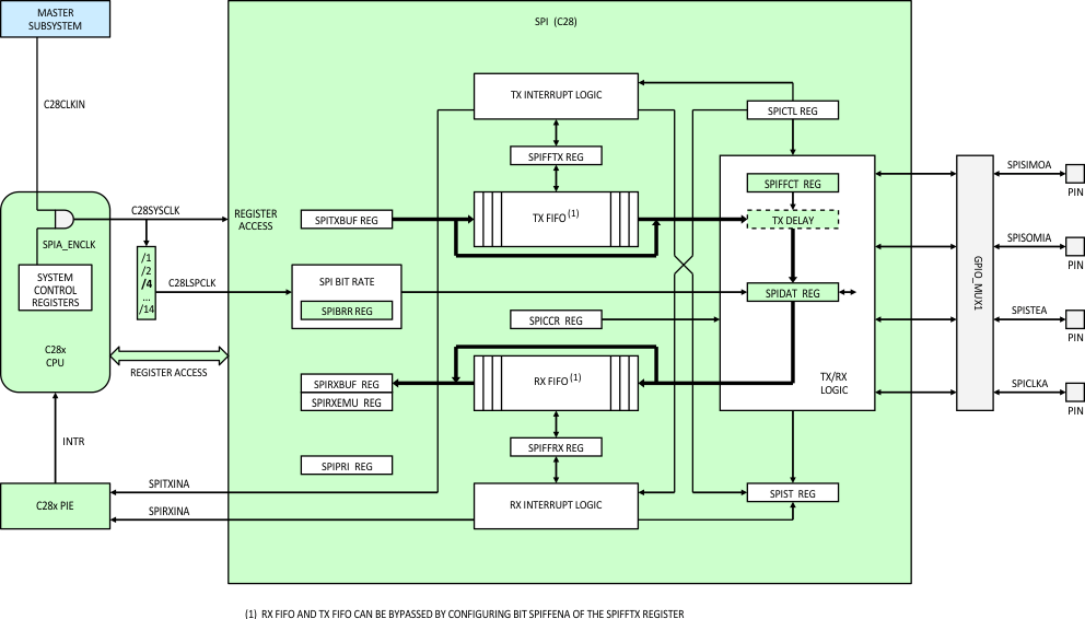 Figure 5-51 SPI (C28x)
5.12.6.1 Functional Overview
The SPI operates in master or slave mode. The master initiates data transfer by sending the SPICLK signal. For both the slave and the master, data is shifted out of the shift registers on one edge of the SPICLK and latched into the shift register on the opposite SPICLK clock edge. If the CLOCK PHASE bit (SPICTL.3) is high, data is transmitted and received a half-cycle before the SPICLK transition. As a result, both controllers send and receive data simultaneously. The application software determines whether the data is meaningful or dummy data. There are three possible methods for data transmission:
- Master sends data; slave sends dummy data
- Master sends data; slave sends data
- Master sends dummy data; slave sends data
The master can initiate a data transfer at any time because it controls the SPICLK signal. The software, however, determines how the master detects when the slave is ready to broadcast data.
5.12.6.2 SPI Electrical Data and Timing
This section contains both Master Mode and Slave Mode timing data.
5.12.6.2.1 Master Mode Timing
Table 5-75 lists the master mode timing (clock phase = 0) and Table 5-76 lists the timing (clock phase = 1). Figure 5-52 and Figure 5-53 show the timing waveforms.
Table 5-75 SPI Master Mode External Timing (Clock Phase = 0)(1) (2) (3) (4) (5)
| NO. | SPI WHEN (SPIBRR + 1) IS EVEN OR SPIBRR = 0 OR 2 | SPI WHEN (SPIBRR + 1) IS ODD AND SPIBRR > 3 |
UNIT | ||||
|---|---|---|---|---|---|---|---|
| MIN | MAX | MIN | MAX | ||||
| 1 | tc(SPC)M | Cycle time, SPICLK | 4tc(LCO) | 128tc(LCO) | 5tc(LCO) | 127tc(LCO) | ns |
| 2 | tw(SPCH)M | Pulse duration, SPICLK high (clock polarity = 0) |
0.5tc(SPC)M – 10 | 0.5tc(SPC)M | 0.5tc(SPC)M – 0.5tc(LCO) – 10 | 0.5tc(SPC)M – 0.5tc(LCO) | ns |
| tw(SPCL)M | Pulse duration, SPICLK low (clock polarity = 1) |
0.5tc(SPC)M – 10 | 0.5tc(SPC)M | 0.5tc(SPC)M – 0.5tc(LCO) – 10 | 0.5tc(SPC)M – 0.5tc(LCO) | ||
| 3 | tw(SPCL)M | Pulse duration, SPICLK low (clock polarity = 0) |
0.5tc(SPC)M – 10 | 0.5tc(SPC)M | 0.5tc(SPC)M + 0.5tc(LCO) – 10 | 0.5tc(SPC)M + 0.5tc(LCO) | ns |
| tw(SPCH)M | Pulse duration, SPICLK high (clock polarity = 1) |
0.5tc(SPC)M – 10 | 0.5tc(SPC)M | 0.5tc(SPC)M + 0.5tc(LCO) – 10 | 0.5tc(SPC)M + 0.5tc(LCO) | ||
| 4 | td(SPCH-SIMO)M | Delay time, SPICLK high to SPISIMO valid (clock polarity = 0) | 10 | 10 | ns | ||
| td(SPCL-SIMO)M | Delay time, SPICLK low to SPISIMO valid (clock polarity = 1) | 10 | 10 | ||||
| 5 | tv(SPCL-SIMO)M | Valid time, SPISIMO data valid after SPICLK low (clock polarity = 0) | 0.5tc(SPC)M – 10 | 0.5tc(SPC)M + 0.5tc(LCO) – 10 | ns | ||
| tv(SPCH-SIMO)M | Valid time, SPISIMO data valid after SPICLK high (clock polarity = 1) | 0.5tc(SPC)M – 10 | 0.5tc(SPC)M + 0.5tc(LCO) – 10 | ||||
| 8 | tsu(SOMI-SPCL)M | Setup time, SPISOMI before SPICLK low (clock polarity = 0) | 35 | 35 | ns | ||
| tsu(SOMI-SPCH)M | Setup time, SPISOMI before SPICLK high (clock polarity = 1) | 35 | 35 | ||||
| 9 | tv(SPCL-SOMI)M | Valid time, SPISOMI data valid after SPICLK low (clock polarity = 0) | 0.25tc(SPC)M – 10 | 0.5tc(SPC)M – 0.5tc(LCO) – 10 | ns | ||
| tv(SPCH-SOMI)M | Valid time, SPISOMI data valid after SPICLK high (clock polarity = 1) | 0.25tc(SPC)M – 10 | 0.5tc(SPC)M – 0.5tc(LCO) – 10 | ||||
Master mode transmit 25-MHz MAX, master mode receive 12.5-MHz MAX
Slave mode transmit 12.5-MHz MAX, slave mode receive 12.5-MHz MAX.
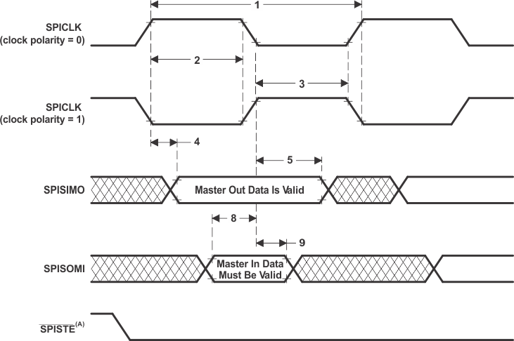
Table 5-76 SPI Master Mode External Timing (Clock Phase = 1)(1) (2) (3) (4) (5)
| NO. | SPI WHEN (SPIBRR + 1) IS EVEN OR SPIBRR = 0 OR 2 | SPI WHEN (SPIBRR + 1) IS ODD AND SPIBRR > 3 |
UNIT | ||||
|---|---|---|---|---|---|---|---|
| MIN | MAX | MIN | MAX | ||||
| 1 | tc(SPC)M | Cycle time, SPICLK | 4tc(LCO) | 128tc(LCO) | 5tc(LCO) | 127tc(LCO) | ns |
| 2 | tw(SPCH)M | Pulse duration, SPICLK high (clock polarity = 0) |
0.5tc(SPC)M – 10 | 0.5tc(SPC)M | 0.5tc(SPC)M – 0.5tc(LCO) – 10 | 0.5tc(SPC)M – 0.5tc(LCO) | ns |
| tw(SPCL))M | Pulse duration, SPICLK low (clock polarity = 1) |
0.5tc(SPC)M – 10 | 0.5tc(SPC)M | 0.5tc(SPC)M – 0.5tc(LCO) – 10 | 0.5tc(SPC)M – 0.5tc(LCO) | ||
| 3 | tw(SPCL)M | Pulse duration, SPICLK low (clock polarity = 0) |
0.5tc(SPC)M – 10 | 0.5tc(SPC)M | 0.5tc(SPC)M + 0.5tc(LCO) – 10 | 0.5tc(SPC)M + 0.5tc(LCO) | ns |
| tw(SPCH)M | Pulse duration, SPICLK high (clock polarity = 1) |
0.5tc(SPC)M – 10 | 0.5tc(SPC)M | 0.5tc(SPC)M + 0.5tc(LCO) – 10 | 0.5tc(SPC)M + 0.5tc(LCO) | ||
| 6 | tsu(SIMO-SPCH)M | Setup time, SPISIMO data valid before SPICLK high (clock polarity = 0) | 0.5tc(SPC)M – 10 | 0.5tc(SPC)M – 10 | ns | ||
| tsu(SIMO-SPCL)M | Setup time, SPISIMO data valid before SPICLK low (clock polarity = 1) | 0.5tc(SPC)M – 10 | 0.5tc(SPC)M – 10 | ||||
| 7 | tv(SPCH-SIMO)M | Valid time, SPISIMO data valid after SPICLK high (clock polarity = 0) | 0.5tc(SPC)M – 10 | 0.5tc(SPC)M – 10 | ns | ||
| tv(SPCL-SIMO)M | Valid time, SPISIMO data valid after SPICLK low (clock polarity = 1) | 0.5tc(SPC)M – 10 | 0.5tc(SPC)M – 10 | ||||
| 10 | tsu(SOMI-SPCH)M | Setup time, SPISOMI before SPICLK high (clock polarity = 0) | 35 | 35 | ns | ||
| tsu(SOMI-SPCL)M | Setup time, SPISOMI before SPICLK low (clock polarity = 1) | 35 | 35 | ||||
| 11 | tv(SPCH-SOMI)M | Valid time, SPISOMI data valid after SPICLK high (clock polarity = 0) | 0.25tc(SPC)M – 10 | 0.5tc(SPC)M – 10 | ns | ||
| tv(SPCL-SOMI)M | Valid time, SPISOMI data valid after SPICLK low (clock polarity = 1) | 0.25tc(SPC)M – 10 | 0.5tc(SPC)M – 10 | ||||
Master mode transmit 25-MHz MAX, master mode receive 12.5 MHz MAX
Slave mode transmit 12.5-MHz MAX, slave mode receive 12.5 MHz MAX.
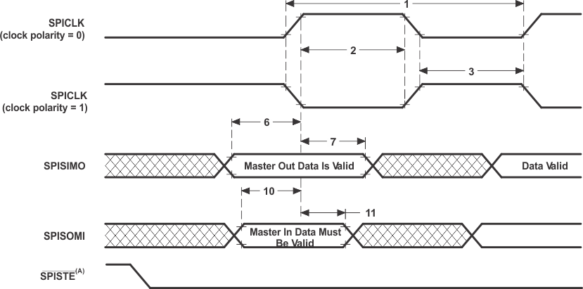
5.12.6.2.2 SPI Slave Mode Timing
Table 5-77 lists the slave mode external timing (clock phase = 0) and Table 5-78 (clock phase = 1). Figure 5-54 and Figure 5-55 show the timing waveforms.
Table 5-77 SPI Slave Mode External Timing (Clock Phase = 0)(1) (2) (4) (3) (5)
| NO. | MIN | MAX | UNIT | ||
|---|---|---|---|---|---|
| 12 | tc(SPC)S | Cycle time, SPICLK | 4tc(LCO) | ns | |
| 13 | tw(SPCH)S | Pulse duration, SPICLK high (clock polarity = 0) | 0.5tc(SPC)S – 10 | 0.5tc(SPC)S | ns |
| tw(SPCL)S | Pulse duration, SPICLK low (clock polarity = 1) | 0.5tc(SPC)S – 10 | 0.5tc(SPC)S | ||
| 14 | tw(SPCL)S | Pulse duration, SPICLK low (clock polarity = 0) | 0.5tc(SPC)S – 10 | 0.5tc(SPC)S | ns |
| tw(SPCH)S | Pulse duration, SPICLK high (clock polarity = 1) | 0.5tc(SPC)S – 10 | 0.5tc(SPC)S | ||
| 15 | td(SPCH-SOMI)S | Delay time, SPICLK high to SPISOMI valid (clock polarity = 0) | 35 | ns | |
| td(SPCL-SOMI)S | Delay time, SPICLK low to SPISOMI valid (clock polarity = 1) | 35 | |||
| 16 | tv(SPCL-SOMI)S | Valid time, SPISOMI data valid after SPICLK low (clock polarity = 0) |
0.75tc(SPC)S | ns | |
| tv(SPCH-SOMI)S | Valid time, SPISOMI data valid after SPICLK high (clock polarity = 1) |
0.75tc(SPC)S | |||
| 19 | tsu(SIMO-SPCL)S | Setup time, SPISIMO before SPICLK low (clock polarity = 0) | 35 | ns | |
| tsu(SIMO-SPCH)S | Setup time, SPISIMO before SPICLK high (clock polarity = 1) | 35 | |||
| 20 | tv(SPCL-SIMO)S | Valid time, SPISIMO data valid after SPICLK low (clock polarity = 0) |
0.5tc(SPC)S – 10 | ns | |
| tv(SPCH-SIMO)S | Valid time, SPISIMO data valid after SPICLK high (clock polarity = 1) |
0.5tc(SPC)S – 10 | |||
Master mode transmit 25-MHz MAX, master mode receive 12.5-MHz MAX
Slave mode transmit 12.5-MHz MAX, slave mode receive 12.5-MHz MAX.
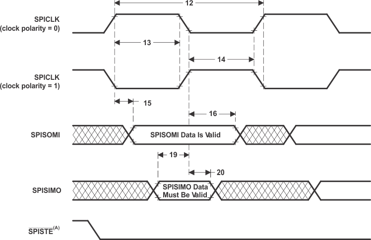
Table 5-78 SPI Slave Mode External Timing (Clock Phase = 1)(1) (2) (3) (4)
| NO. | MIN | MAX | UNIT | ||
|---|---|---|---|---|---|
| 12 | tc(SPC)S | Cycle time, SPICLK | 8tc(LCO) | ns | |
| 13 | tw(SPCH)S | Pulse duration, SPICLK high (clock polarity = 0) | 0.5tc(SPC)S – 10 | 0.5tc(SPC)S | ns |
| tw(SPCL)S | Pulse duration, SPICLK low (clock polarity = 1) | 0.5tc(SPC)S – 10 | 0.5tc(SPC)S | ||
| 14 | tw(SPCL)S | Pulse duration, SPICLK low (clock polarity = 0) | 0.5tc(SPC)S – 10 | 0.5tc(SPC)S | ns |
| tw(SPCH)S | Pulse duration, SPICLK high (clock polarity = 1) | 0.5tc(SPC)S – 10 | 0.5tc(SPC)S | ||
| 17 | tsu(SOMI-SPCH)S | Setup time, SPISOMI before SPICLK high (clock polarity = 0) | 0.125tc(SPC)S | ns | |
| tsu(SOMI-SPCL)S | Setup time, SPISOMI before SPICLK low (clock polarity = 1) | 0.125tc(SPC)S | |||
| 18 | tv(SPCL-SOMI)S | Valid time, SPISOMI data valid after SPICLK low (clock polarity = 1) |
0.75tc(SPC)S | ns | |
| tv(SPCH-SOMI)S | Valid time, SPISOMI data valid after SPICLK high (clock polarity = 0) |
0.75tc(SPC)S | |||
| 21 | tsu(SIMO-SPCH)S | Setup time, SPISIMO before SPICLK high (clock polarity = 0) | 35 | ns | |
| tsu(SIMO-SPCL)S | Setup time, SPISIMO before SPICLK low (clock polarity = 1) | 35 | |||
| 22 | tv(SPCH-SIMO)S | Valid time, SPISIMO data valid after SPICLK high (clock polarity = 0) |
0.5tc(SPC)S – 10 | ns | |
| tv(SPCL-SIMO)S | Valid time, SPISIMO data valid after SPICLK low (clock polarity = 1) |
0.5tc(SPC)S – 10 | |||
Master mode transmit 25-MHz MAX, master mode receive 12.5-MHz MAX
Slave mode transmit 12.5-MHz MAX, slave mode receive 12.5-MHz MAX.
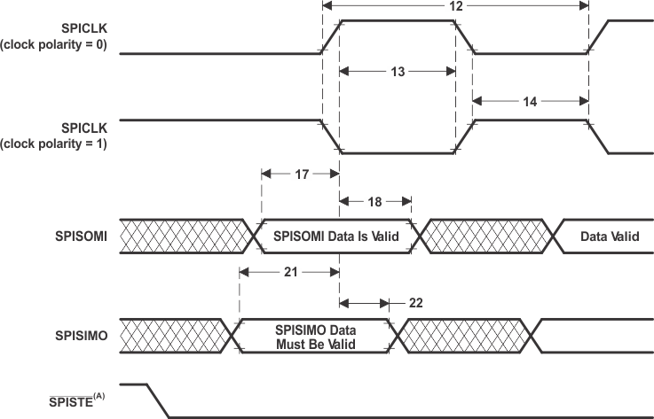
5.12.7 C28x Multichannel Buffered Serial Port
This device provides one high-speed McBSP that allows direct interface to codecs and other devices. The CPU accesses data, control, and status information. The MCBSP also supports µDMA transfers.
The McBSP consists of a data-flow path and a control path connected to external devices by six pins. Data is communicated to devices interfaced with the McBSP via the data transmit (DX) pin for transmission and via the data receive (DR) pin for reception. Control information in the form of clocking and frame synchronization is communicated via the following pins: CLKX (transmit clock), CLKR (receive clock), FSX (transmit frame synchronization), and FSR (receive frame synchronization).
The CPU and the DMA controller communicate with the McBSP through 16-bit-wide registers accessible via the internal peripheral bus. The CPU or the DMA controller writes the data to be transmitted to the data transmit registers (DXR1, DXR2). Data written to the DXRs is shifted out to DX via the transmit shift registers (XSR1, XSR2). Similarly, receive data on the DR pin is shifted into the receive shift registers (RSR1, RSR2) and copied into the receive buffer registers (RBR1, RBR2). The contents of the RBRs is then copied to the DRRs, which can be read by the CPU or the DMA controller. This method allows simultaneous movement of internal and external data communications.
DRR2, RBR2, RSR2, DXR2, and XSR2 are not used (written, read, or shifted) if the serial word length is 8 bits, 12 bits, or 16 bits. For larger word lengths, these registers are needed to hold the most significant bits.
The frame and clock loop-back is implemented at chip level to enable CLKX and FSX to drive CLKR and FSR. If the loop-back is enabled, the CLKR and FSR get their signals from the CLKX and FSX pads instead of the CLKR and FSR pins.
McBSP features include:
- Full-duplex communication
- Double-buffered transmission and triple-buffered reception, allowing a continuous data stream
- Independent clocking and framing for reception and transmission
- The capability to send interrupts to the CPU and to send DMA events to the DMA controller
- 128 channels for transmission and reception
- Multichannel selection modes that enable or disable block transfers in each of the channels
- Direct interface to industry-standard codecs, analog interface chips (AICs), and other serially connected A/D and D/A devices
- Support for external generation of clock signals and frame-synchronization signals
- A programmable sample rate generator for internal generation and control of clock signals and frame synchronization signals
- Programmable polarity for frame-synchronization pulses and clock signals
- Direct interface to:
- T1/E1 framers
- IOM-2 compliant devices
- AC97-compliant devices (the necessary multi-phase frame capability is provided)
- I2S compliant devices
- SPI devices
- A wide selection of data sizes: 8, 12, 16, 20, 24, and 32 bits
NOTE
A value of the chosen data size is referred to as a serial word or word in this section. Elsewhere, word is used to describe a 16-bit value.
- µ-law and A-law companding
- The option of transmitting/receiving 8-bit data with the LSB first
- Status bits for flagging exception/error conditions
- ABIS mode is not supported
Figure 5-56 shows the C28x McBSP peripheral.
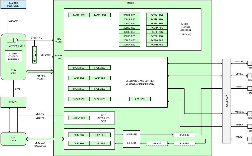 Figure 5-56 McBSP (C28x)
5.12.7.1 McBSP Electrical Data and Timing
5.12.7.1.1 McBSP Transmit and Receive Timing
Table 5-79 McBSP Timing Requirements(1) (2)
| NO. | MIN | MAX | UNIT | |||
|---|---|---|---|---|---|---|
| McBSP module clock (CLKG, CLKX, CLKR) range | 1 | kHz | ||||
| 25 (3) | MHz | |||||
| McBSP module cycle time (CLKG, CLKX, CLKR) range | 40 | ns | ||||
| 1 | ms | |||||
| M11 | tc(CKRX) | Cycle time, CLKR/X | CLKR/X ext | 2P | ns | |
| M12 | tw(CKRX) | Pulse duration, CLKR/X high or CLKR/X low | CLKR/X ext | P – 7 | ns | |
| M13 | tr(CKRX) | Rise time, CLKR/X | CLKR/X ext | 7 | ns | |
| M14 | tf(CKRX) | Fall time, CLKR/X | CLKR/X ext | 7 | ns | |
| M15 | tsu(FRH-CKRL) | Setup time, external FSR high before CLKR low | CLKR int | 18 | ns | |
| CLKR ext | 2 | |||||
| M16 | th(CKRL-FRH) | Hold time, external FSR high after CLKR low | CLKR int | 0 | ns | |
| CLKR ext | 6 | |||||
| M17 | tsu(DRV-CKRL) | Setup time, DR valid before CLKR low | CLKR int | 18 | ns | |
| CLKR ext | 5 | |||||
| M18 | th(CKRL-DRV) | Hold time, DR valid after CLKR low | CLKR int | 0 | ns | |
| CLKR ext | 3 | |||||
| M19 | tsu(FXH-CKXL) | Setup time, external FSX high before CLKX low | CLKX int | 18 | ns | |
| CLKX ext | 2 | |||||
| M20 | th(CKXL-FXH) | Hold time, external FSX high after CLKX low | CLKX int | 0 | ns | |
| CLKX ext | 6 | |||||
Table 5-80 McBSP Switching Characteristics(1) (2)
over recommended operating conditions (unless otherwise noted)| NO. | PARAMETER | MIN | MAX | UNIT | |||
|---|---|---|---|---|---|---|---|
| M1 | tc(CKRX) | Cycle time, CLKR/X | CLKR/X int | 2P | ns | ||
| M2 | tw(CKRXH) | Pulse duration, CLKR/X high | CLKR/X int | D – 5 (3) | D + 5 (3) | ns | |
| M3 | tw(CKRXL) | Pulse duration, CLKR/X low | CLKR/X int | C – 5 (3) | C + 5 (3) | ns | |
| M4 | td(CKRH-FRV) | Delay time, CLKR high to internal FSR valid | CLKR int | 0 | 4 | ns | |
| CLKR ext | 3 | 27 | |||||
| M5 | td(CKXH-FXV) | Delay time, CLKX high to internal FSX valid | CLKX int | 0 | 4 | ns | |
| CLKX ext | 3 | 27 | |||||
| M6 | tdis(CKXH-DXHZ) | Disable time, CLKX high to DX high impedance following last data bit | CLKX int | 8 | ns | ||
| CLKX ext | 14 | ||||||
| M7 | td(CKXH-DXV) | Delay time, CLKX high to DX valid. | CLKX int | 9 | ns | ||
| This applies to all bits except the first bit transmitted. | CLKX ext | 28 | |||||
| Delay time, CLKX high to DX valid | DXENA = 0 | CLKX int | 8 | ||||
| CLKX ext | 14 | ||||||
| Only applies to first bit transmitted when in Data Delay 1 or 2 (XDATDLY=01b or 10b) modes | DXENA = 1 | CLKX int | P + 8 | ||||
| CLKX ext | P + 14 | ||||||
| M8 | ten(CKXH-DX) | Enable time, CLKX high to DX driven | DXENA = 0 | CLKX int | 0 | ns | |
| CLKX ext | 6 | ||||||
| Only applies to first bit transmitted when in Data Delay 1 or 2 (XDATDLY=01b or 10b) modes | DXENA = 1 | CLKX int | P | ||||
| CLKX ext | P + 6 | ||||||
| M9 | td(FXH-DXV) | Delay time, FSX high to DX valid | DXENA = 0 | FSX int | 8 | ns | |
| FSX ext | 14 | ||||||
| Only applies to first bit transmitted when in Data Delay 0 (XDATDLY=00b) mode. | DXENA = 1 | FSX int | P + 8 | ||||
| FSX ext | P + 14 | ||||||
| M10 | ten(FXH-DX) | Enable time, FSX high to DX driven | DXENA = 0 | FSX int | 0 | ns | |
| FSX ext | 6 | ||||||
| Only applies to first bit transmitted when in Data Delay 0 (XDATDLY=00b) mode | DXENA = 1 | FSX int | P | ||||
| FSX ext | P + 6 | ||||||
D = CLKRX high pulse width = P
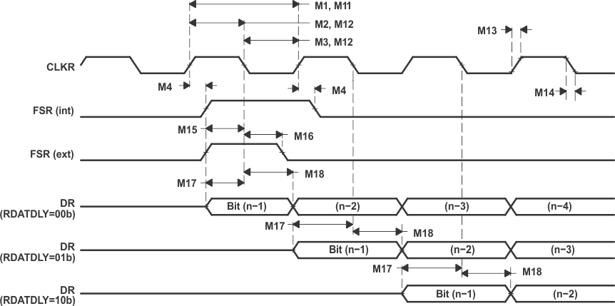 Figure 5-57 McBSP Receive Timing
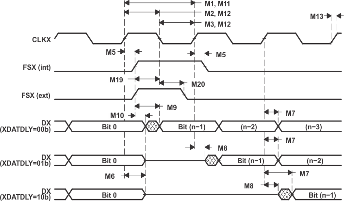 Figure 5-58 McBSP Transmit Timing
5.12.7.1.2 McBSP as SPI Master or Slave Timing
Table 5-81 McBSP as SPI Master or Slave Timing Requirements (CLKSTP = 10b, CLKXP = 0)(1)
| NO. | MASTER | SLAVE | UNIT | ||||
|---|---|---|---|---|---|---|---|
| MIN | MAX | MIN | MAX | ||||
| M30 | tsu(DRV-CKXL) | Setup time, DR valid before CLKX low | 30 | 8P – 10 | ns | ||
| M31 | th(CKXL-DRV) | Hold time, DR valid after CLKX low | 1 | 8P – 10 | ns | ||
| M32 | tsu(BFXL-CKXH) | Setup time, FSX low before CLKX high | 8P + 10 | ns | |||
| M33 | tc(CKX) | Cycle time, CLKX | 2P(2) | 16P | ns | ||
Table 5-82 McBSP as SPI Master or Slave Switching Characteristics Over Recommended Operating Conditions (Unless Otherwise Noted) (CLKSTP = 10b, CLKXP = 0)
| NO. | PARAMETER | MASTER | SLAVE | UNIT | |||
|---|---|---|---|---|---|---|---|
| MIN | MAX | MIN | MAX | ||||
| M24 | th(CKXL-FXL) | Hold time, FSX low after CLKX low | 2P(1) | ns | |||
| M25 | td(FXL-CKXH) | Delay time, FSX low to CLKX high | P | ns | |||
| M28 | tdis(FXH-DXHZ) | Disable time, DX high impedance following last data bit from FSX high | 6 | 6P + 6 | ns | ||
| M29 | td(FXL-DXV) | Delay time, FSX low to DX valid | 6 | 4P + 6 | ns | ||
 Figure 5-59 McBSP Timing as SPI Master or Slave: CLKSTP = 10b, CLKXP = 0
Table 5-83 McBSP as SPI Master or Slave Timing Requirements (CLKSTP = 11b, CLKXP = 0)(1)
| NO. | MASTER | SLAVE | UNIT | ||||
|---|---|---|---|---|---|---|---|
| MIN | MAX | MIN | MAX | ||||
| M39 | tsu(DRV-CKXH) | Setup time, DR valid before CLKX high | 30 | 8P – 10 | ns | ||
| M40 | th(CKXH-DRV) | Hold time, DR valid after CLKX high | 1 | 8P – 10 | ns | ||
| M41 | tsu(FXL-CKXH) | Setup time, FSX low before CLKX high | 16P + 10 | ns | |||
| M42 | tc(CKX) | Cycle time, CLKX | 2P(2) | 16P | ns | ||
Table 5-84 McBSP as SPI Master or Slave Switching Characteristics Over Recommended Operating Conditions (Unless Otherwise Noted) (CLKSTP = 11b, CLKXP = 0)
| NO. | PARAMETER | MASTER | SLAVE | UNIT | |||
|---|---|---|---|---|---|---|---|
| MIN | MAX | MIN | MAX | ||||
| M34 | th(CKXL-FXL) | Hold time, FSX low after CLKX low | P | ns | |||
| M35 | td(FXL-CKXH) | Delay time, FSX low to CLKX high | 2P(1) | ns | |||
| M37 | tdis(CKXL-DXHZ) | Disable time, DX high impedance following last data bit from CLKX low | P + 6 | 7P + 6 | ns | ||
| M38 | td(FXL-DXV) | Delay time, FSX low to DX valid | 6 | 4P + 6 | ns | ||
 Figure 5-60 McBSP Timing as SPI Master or Slave: CLKSTP = 11b, CLKXP = 0
Table 5-85 McBSP as SPI Master or Slave Timing Requirements (CLKSTP = 10b, CLKXP = 1)(1)
| NO. | MASTER | SLAVE | UNIT | ||||
|---|---|---|---|---|---|---|---|
| MIN | MAX | MIN | MAX | ||||
| M49 | tsu(DRV-CKXH) | Setup time, DR valid before CLKX high | 30 | 8P – 10 | ns | ||
| M50 | th(CKXH-DRV) | Hold time, DR valid after CLKX high | 1 | 8P – 10 | ns | ||
| M51 | tsu(FXL-CKXL) | Setup time, FSX low before CLKX low | 8P + 10 | ns | |||
| M52 | tc(CKX) | Cycle time, CLKX | 2P(2) | 16P | ns | ||
Table 5-86 McBSP as SPI Master or Slave Switching Characteristics Over Recommended Operating Conditions (Unless Otherwise Noted) (CLKSTP = 10b, CLKXP = 1)
| NO. | PARAMETER | MASTER | SLAVE | UNIT | |||
|---|---|---|---|---|---|---|---|
| MIN | MAX | MIN | MAX | ||||
| M43 | th(CKXH-FXL) | Hold time, FSX low after CLKX high | 2P(1) | ns | |||
| M44 | td(FXL-CKXL) | Delay time, FSX low to CLKX low | P | ns | |||
| M47 | tdis(FXH-DXHZ) | Disable time, DX high impedance following last data bit from FSX high | 6 | 6P + 6 | ns | ||
| M48 | td(FXL-DXV) | Delay time, FSX low to DX valid | 6 | 4P + 6 | ns | ||
 Figure 5-61 McBSP Timing as SPI Master or Slave: CLKSTP = 10b, CLKXP = 1
Table 5-87 McBSP as SPI Master or Slave Timing Requirements (CLKSTP = 11b, CLKXP = 1)(1)
| NO. | MASTER | SLAVE | UNIT | ||||
|---|---|---|---|---|---|---|---|
| MIN | MAX | MIN | MAX | ||||
| M58 | tsu(DRV-CKXL) | Setup time, DR valid before CLKX low | 30 | 8P – 10 | ns | ||
| M59 | th(CKXL-DRV) | Hold time, DR valid after CLKX low | 1 | 8P – 10 | ns | ||
| M60 | tsu(FXL-CKXL) | Setup time, FSX low before CLKX low | 16P + 10 | ns | |||
| M61 | tc(CKX) | Cycle time, CLKX | 2P(2) | 16P | ns | ||
Table 5-88 McBSP as SPI Master or Slave Switching Characteristics Over Recommended Operating Conditions (Unless Otherwise Noted) (CLKSTP = 11b, CLKXP = 1)(1)
| NO. | PARAMETER | MASTER(2) | SLAVE | UNIT | |||
|---|---|---|---|---|---|---|---|
| MIN | MAX | MIN | MAX | ||||
| M53 | th(CKXH-FXL) | Hold time, FSX low after CLKX high | P | ns | |||
| M54 | td(FXL-CKXL) | Delay time, FSX low to CLKX low | 2P(1) | ns | |||
| M55 | td(CLKXH-DXV) | Delay time, CLKX high to DX valid | –2 | 0 | 3P + 6 | 5P + 20 | ns |
| M56 | tdis(CKXH-DXHZ) | Disable time, DX high impedance following last data bit from CLKX high | P + 6 | 7P + 6 | ns | ||
| M57 | td(FXL-DXV) | Delay time, FSX low to DX valid | 6 | 4P + 6 | ns | ||
D = CLKX high pulse width = P
 Figure 5-62 McBSP Timing as SPI Master or Slave: CLKSTP = 11b, CLKXP = 1