ZHCSF09 May 2016 FDC2112-Q1 , FDC2114-Q1 , FDC2212-Q1 , FDC2214-Q1
PRODUCTION DATA.
- 1 特性
- 2 应用
- 3 说明
- 4 修订历史记录
- 5 Pin Configuration and Functions
- 6 Specifications
-
7 Detailed Description
- 7.1 Overview
- 7.2 Functional Block Diagrams
- 7.3 Feature Description
- 7.4 Device Functional Modes
- 7.5 Programming
- 7.6
Register Maps
- 7.6.1 Register List
- 7.6.2 Address 0x00, DATA_CH0
- 7.6.3 Address 0x01, DATA_LSB_CH0 (FDC2212 / FDC2214 only)
- 7.6.4 Address 0x02, DATA_CH1
- 7.6.5 Address 0x03, DATA_LSB_CH1 (FDC2212 / FDC2214 only)
- 7.6.6 Address 0x04, DATA_CH2 (FDC2114, FDC2214 only)
- 7.6.7 Address 0x05, DATA_LSB_CH2 (FDC2214 only)
- 7.6.8 Address 0x06, DATA_CH3 (FDC2114, FDC2214 only)
- 7.6.9 Address 0x07, DATA_LSB_CH3 (FDC2214 only)
- 7.6.10 Address 0x08, RCOUNT_CH0
- 7.6.11 Address 0x09, RCOUNT_CH1
- 7.6.12 Address 0x0A, RCOUNT_CH2 (FDC2114, FDC2214 only)
- 7.6.13 Address 0x0B, RCOUNT_CH3 (FDC2114, FDC2214 only)
- 7.6.14 Address 0x0C, OFFSET_CH0 (FDC21112 / FDC2114 only)
- 7.6.15 Address 0x0D, OFFSET_CH1 (FDC21112 / FDC2114 only)
- 7.6.16 Address 0x0E, OFFSET_CH2 (FDC2114 only)
- 7.6.17 Address 0x0F, OFFSET_CH3 (FDC2114 only)
- 7.6.18 Address 0x10, SETTLECOUNT_CH0
- 7.6.19 Address 0x11, SETTLECOUNT_CH1
- 7.6.20 Address 0x12, SETTLECOUNT_CH2 (FDC2114, FDC2214 only)
- 7.6.21 Address 0x13, SETTLECOUNT_CH3 (FDC2114, FDC2214 only)
- 7.6.22 Address 0x14, CLOCK_DIVIDERS_CH0
- 7.6.23 Address 0x15, CLOCK_DIVIDERS_CH1
- 7.6.24 Address 0x16, CLOCK_DIVIDERS_CH2 (FDC2114, FDC2214 only)
- 7.6.25 Address 0x17, CLOCK_DIVIDERS_CH3 (FDC2114, FDC2214 only)
- 7.6.26 Address 0x18, STATUS
- 7.6.27 Address 0x19, ERROR_CONFIG
- 7.6.28 Address 0x1A, CONFIG
- 7.6.29 Address 0x1B, MUX_CONFIG
- 7.6.30 Address 0x1C, RESET_DEV
- 7.6.31 Address 0x1E, DRIVE_CURRENT_CH0
- 7.6.32 Address 0x1F, DRIVE_CURRENT_CH1
- 7.6.33 Address 0x20, DRIVE_CURRENT_CH2 (FDC2114 / FDC2214 only)
- 7.6.34 Address 0x21, DRIVE_CURRENT_CH3 (FDC2114 / FDC2214 only)
- 7.6.35 Address 0x7E, MANUFACTURER_ID
- 7.6.36 Address 0x7F, DEVICE_ID
- 8 Application and Implementation
- 9 Power Supply Recommendations
- 10Layout
- 11器件和文档支持
- 12机械、封装和可订购信息
10 Layout
10.1 Layout Guidelines
- Avoid long traces to connect the sensor to the FDC. Short traces reduce parasitic capacitances between sensor inductor and offer higher system performance.
- Systems that require matched channel response need to have matched trace length on all active channels.
10.2 Layout Examples
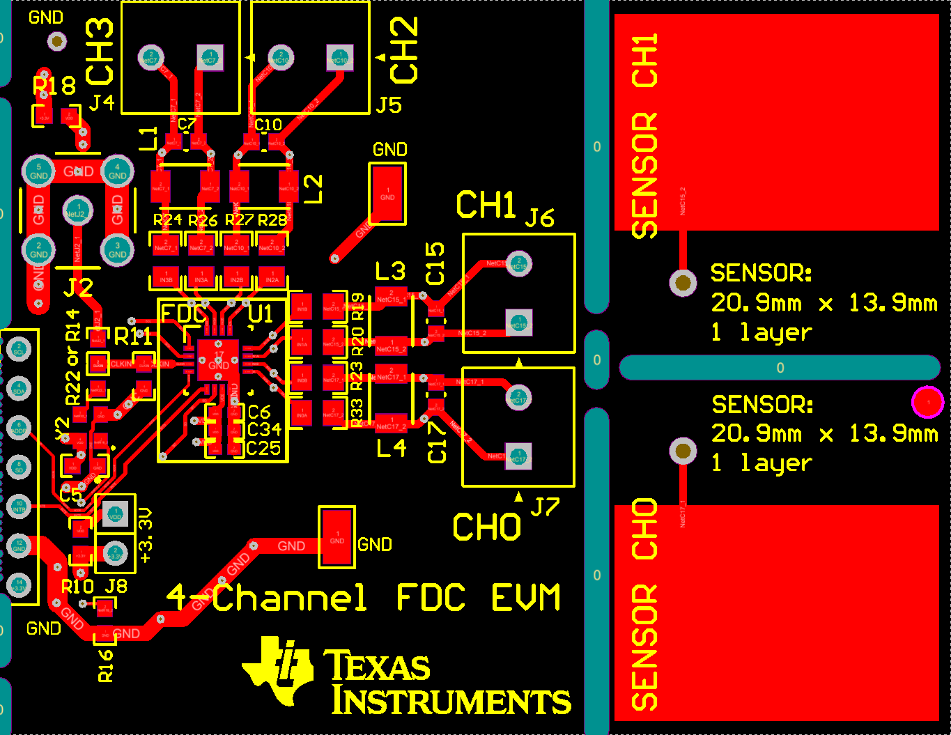
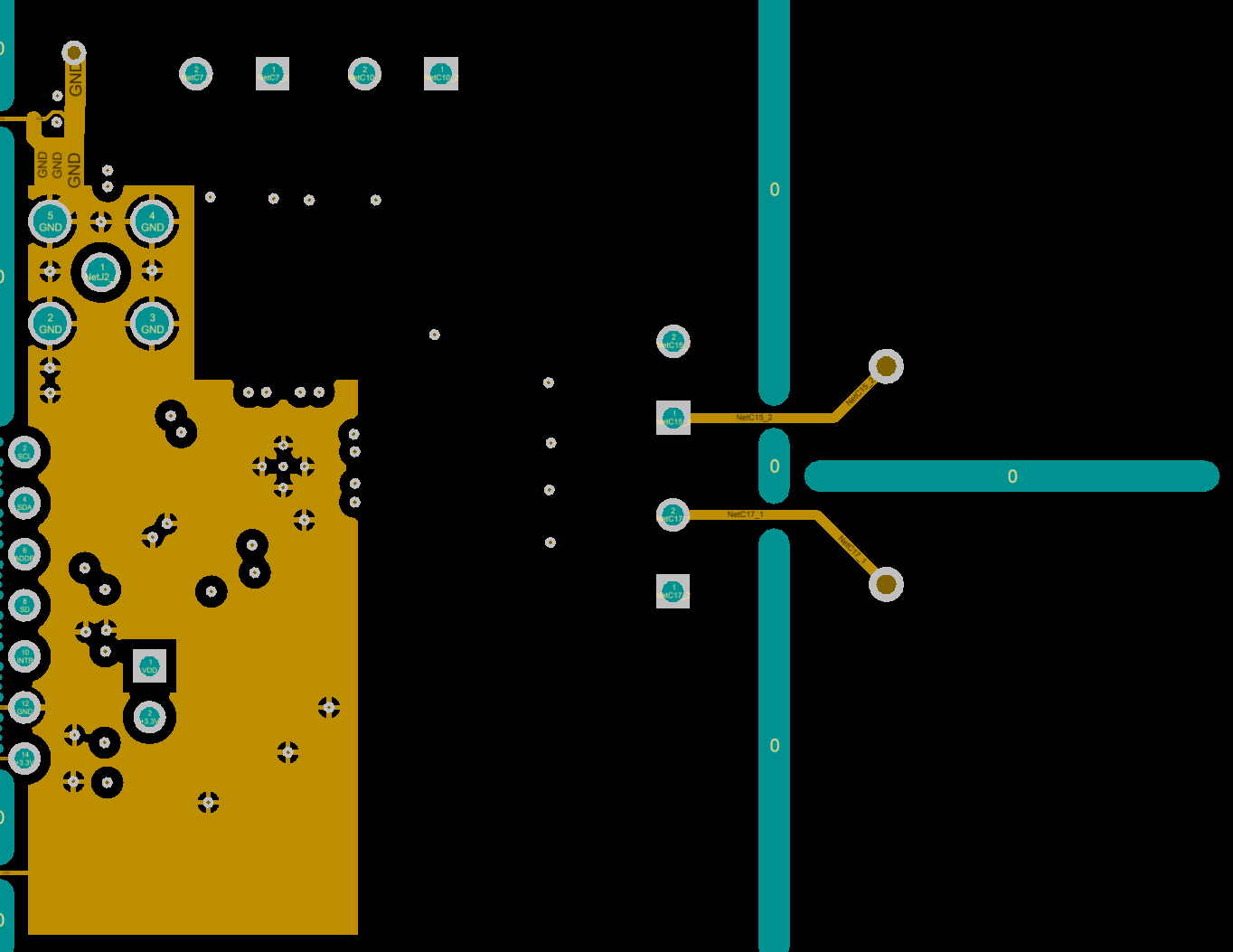
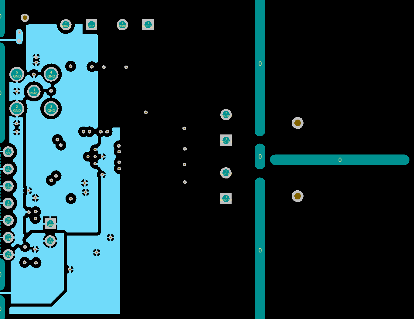
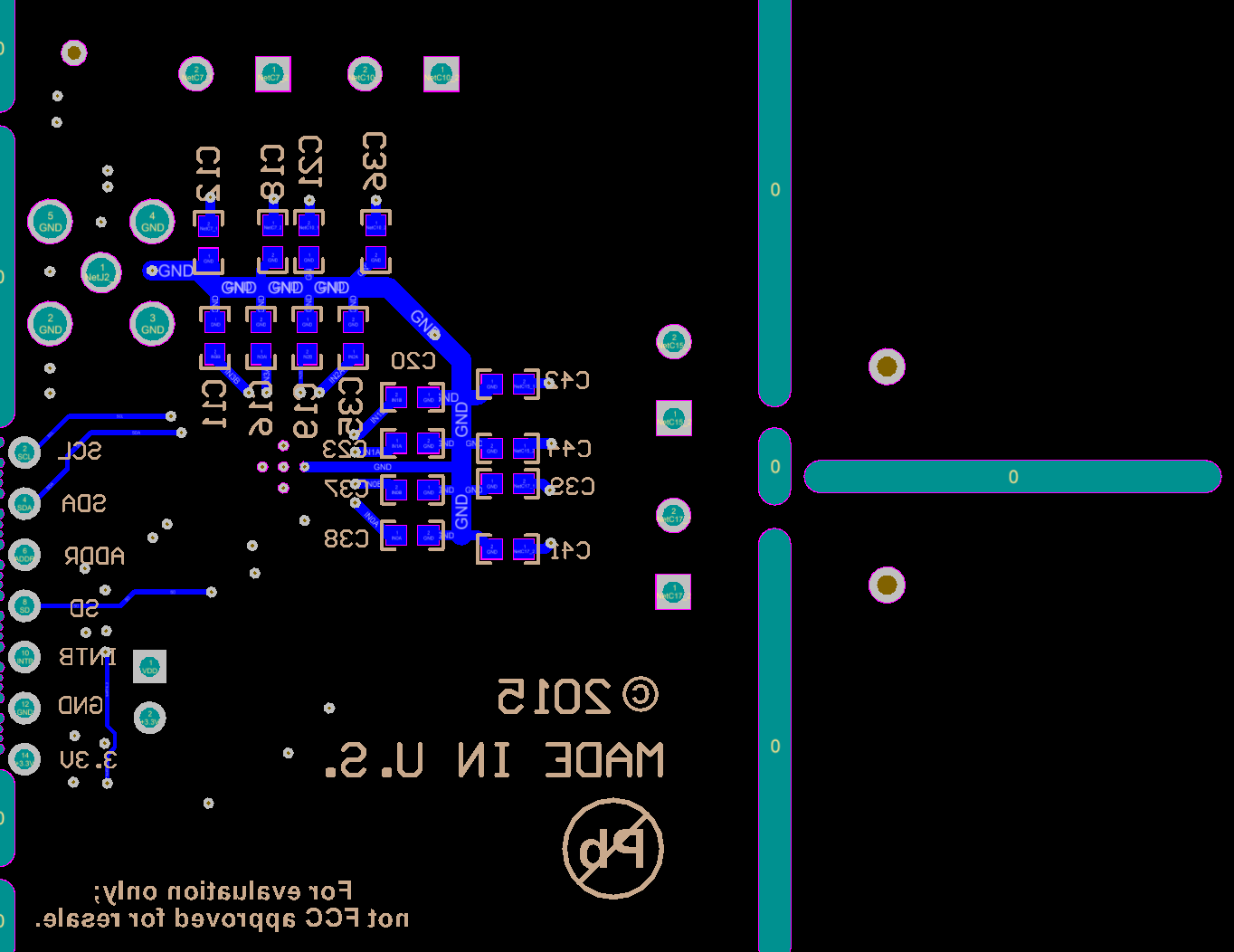
Figure 62 to Figure 65 show the FDC2114 / FDC2214 evaluation module (EVM) layout.
 Figure 62. Example PCB Layout: Top Layer (Signal)
 Figure 63. Example PCB Layout: Mid-Layer 1 (GND)
 Figure 64. Example PCB Layout: Mid-layer 2 (Power)
 Figure 65. Example PCB Layout: Bottom Layer (Signal)