ZHCSDX2A June 2015 – June 2015 FDC2112 , FDC2114 , FDC2212 , FDC2214
PRODUCTION DATA.
- 1 特性
- 2 应用
- 3 说明
- 4 修订历史记录
- 5 说明 (续)
- 6 Device Comparison Table
- 7 Pin Configuration and Functions
- 8 Specifications
-
9 Detailed Description
- 9.1 Overview
- 9.2 Functional Block Diagrams
- 9.3 Feature Description
- 9.4 Device Functional Modes
- 9.5 Programming
- 9.6
Register Maps
- 9.6.1 Register List
- 9.6.2 Address 0x00, DATA_CH0
- 9.6.3 Address 0x01, DATA_LSB_CH0 (FDC2212 / FDC2214 only)
- 9.6.4 Address 0x02, DATA_CH1
- 9.6.5 Address 0x03, DATA_LSB_CH1 (FDC2212 / FDC2214 only)
- 9.6.6 Address 0x04, DATA_CH2 (FDC2114, FDC2214 only)
- 9.6.7 Address 0x05, DATA_LSB_CH2 (FDC2214 only)
- 9.6.8 Address 0x06, DATA_CH3 (FDC2114, FDC2214 only)
- 9.6.9 Address 0x07, DATA_LSB_CH3 (FDC2214 only)
- 9.6.10 Address 0x08, RCOUNT_CH0
- 9.6.11 Address 0x09, RCOUNT_CH1
- 9.6.12 Address 0x0A, RCOUNT_CH2 (FDC2114, FDC2214 only)
- 9.6.13 Address 0x0B, RCOUNT_CH3 (FDC2114, FDC2214 only)
- 9.6.14 Address 0x0C, OFFSET_CH0 (FDC21112 / FDC2114 only)
- 9.6.15 Address 0x0D, OFFSET_CH1 (FDC21112 / FDC2114 only)
- 9.6.16 Address 0x0E, OFFSET_CH2 (FDC2114 only)
- 9.6.17 Address 0x0F, OFFSET_CH3 (FDC2114 only)
- 9.6.18 Address 0x10, SETTLECOUNT_CH0
- 9.6.19 Address 0x11, SETTLECOUNT_CH1
- 9.6.20 Address 0x12, SETTLECOUNT_CH2 (FDC2114, FDC2214 only)
- 9.6.21 Address 0x13, SETTLECOUNT_CH3 (FDC2114, FDC2214 only)
- 9.6.22 Address 0x14, CLOCK_DIVIDERS_CH0
- 9.6.23 Address 0x15, CLOCK_DIVIDERS_CH1
- 9.6.24 Address 0x16, CLOCK_DIVIDERS_CH2 (FDC2114, FDC2214 only)
- 9.6.25 Address 0x17, CLOCK_DIVIDERS_CH3 (FDC2114, FDC2214 only)
- 9.6.26 Address 0x18, STATUS
- 9.6.27 Address 0x19, ERROR_CONFIG
- 9.6.28 Address 0x1A, CONFIG
- 9.6.29 Address 0x1B, MUX_CONFIG
- 9.6.30 Address 0x1C, RESET_DEV
- 9.6.31 Address 0x1E, DRIVE_CURRENT_CH0
- 9.6.32 Address 0x1F, DRIVE_CURRENT_CH1
- 9.6.33 Address 0x20, DRIVE_CURRENT_CH2 (FDC2114 / FDC2214 only)
- 9.6.34 Address 0x21, DRIVE_CURRENT_CH3 (FDC2114 / FDC2214 only)
- 9.6.35 Address 0x7E, MANUFACTURER_ID
- 9.6.36 Address 0x7F, DEVICE_ID
- 10Application and Implementation
- 11Power Supply Recommendations
- 12Layout
- 13器件和文档支持
- 14机械、封装和可订购信息
7 Pin Configuration and Functions
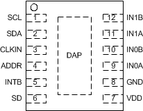
FDC2112/FDC2212 WSON
DNT-12
Top View

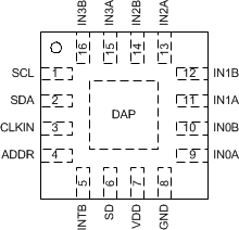
FDC2114/FDC2214 WQFN
RGH-16
Top View

Pin Functions
| PIN | TYPE(1) | DESCRIPTION | |
|---|---|---|---|
| NAME | NO. | ||
| SCL | 1 | I | I2C Clock input |
| SDA | 2 | I/O | I2C Data input/output |
| CLKIN | 3 | I | Master Clock input. Tie this pin to GND if internal oscillator is selected |
| ADDR | 4 | I | I2C Address selection pin: when ADDR=L, I2C address = 0x2A, when ADDR=H, I2C address = 0x2B. |
| INTB | 5 | O | Configurable Interrupt output pin |
| SD | 6 | I | Shutdown input |
| VDD | 7 | P | Power Supply |
| GND | 8 | G | Ground |
| IN0A | 9 | A | Capacitive sensor input 0 |
| IN0B | 10 | A | Capacitive sensor input 0 |
| IN1A | 11 | A | Capacitive sensor input 1 |
| IN1B | 12 | A | Capacitive sensor input 1 |
| IN2A | 13 | A | Capacitive sensor input 2 (FDC2114 / FDC2214 only) |
| IN2B | 14 | A | Capacitive sensor input 2 (FDC2114 / FDC2214 only) |
| IN3A | 15 | A | Capacitive sensor input 3 (FDC2114 / FDC2214 only) |
| IN3B | 16 | A | Capacitive sensor input 3 (FDC2114 / FDC2214 only) |
| DAP(2) | DAP | N/A | Connect to Ground |
(1) I = Input, O = Output, P=Power, G=Ground, A=Analog
(2) There is an internal electrical connection between the exposed Die Attach Pad (DAP) and the GND pin of the device. Although the DAP can be left floating, for best performance the DAP should be connected to the same potential as the device's GND pin. Do not use the DAP as the primary ground for the device. The device GND pin must always be connected to ground.