ZHCSUH8B December 2017 – January 2024 FPC202
PRODUCTION DATA
- 1
- 1 特性
- 2 应用
- 3 说明
- 4 Device Comparison Table
- 5 Pin Configuration and Functions
- 6 Specifications
-
7 Detailed Description
- 7.1 Overview
- 7.2 Functional Block Diagram
- 7.3
Feature Description
- 7.3.1 Host-Side Control Interface
- 7.3.2 LED Control
- 7.3.3 Low-Speed Output Signal Control
- 7.3.4 Low-Speed Input Status and Interrupt Generation
- 7.3.5 Downstream (Port-Side) I2C Master
- 7.3.6 Data Pre-Fetch From Modules
- 7.3.7 Scheduled Write
- 7.3.8 Protocol Timeouts
- 7.3.9 General-Purpose Inputs/Outputs
- 7.3.10 Hot-Plug Support
- 7.4 Device Functional Modes
- 7.5 Programming
- 8 Application and Implementation
- 9 Device and Documentation Support
- 10Revision History
- 11Mechanical, Packaging, and Orderable Information
7.3.2 LED Control
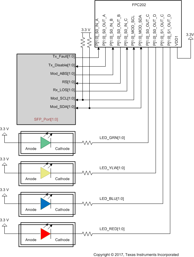
The FPC202 uses four sets of outputs, P[1:0]_S0_OUT_C, P[1:0]_S0_OUT_D, P[1:0]_S1_OUT_C, and P[1:0]_S1_OUT_D to drive LEDs associated with the ports under its control. Most SFP and QSFP applications use one yellow and one green LED per port to indicate different link status such as link up, link down, and other link states. Some QSFP applications require one LED per lane, which equals four LEDs per port.
For applications requiring more than four LEDs per port, spare outputs (OUT_* and GPIO) can be used to drive additional LEDs in a mostly-static fashion. The blinking and dimming capabilities available on the S0_OUT_C, S0_OUT_D, S1_OUT_C, and S1_OUT_D pins are not available on the other FPC202 outputs.
LEDs should be connected to the FPC202 in an active-low fashion as shown in Figure 7-1. When the S0_OUT_C, S0_OUT_D, S1_OUT_C, or S1_OUT_D pin drives a low voltage (VOL), the LED is illuminated. When these pins drive a high voltage (VOH), the LED is off. Bi-color LEDs can be connected in a similar fashion, and each LED should have its own current-limiting resistor. The current-limiting resistor value is selected by choosing the desired maximum current through the LED and the corresponding voltage drop from the LED's current vs. voltage plot. The sum of forward voltage drop of the LED, the voltage drop across the series resistor, and the maximum VOL (0.5 V maximum for currents between 2 and 18 mA) is equal to the LED supply voltage. Note that S0_OUT_C, S0_OUT_D, S1_OUT_C, and S1_OUT_D are tri-stated while the device is held in reset (during POR or while the EN pin is low), and are enabled during normal operation and drive a high voltage by default.
 Figure 7-1 Example Connection Between S0_OUT_C, S0_OUT_D, S1_OUT_C, and S1_OUT_D and Active-Low LEDs
Each port under the FPC202’s control has a set of registers that allow the user to configure each LED into one of the following states:
- ON
- OFF
- PWM (ON with programmable intensity)
- BLINK (with programmable blink duty cycle, frequency, and ON intensity)
LED blinking can be synchronized across both ports under the FPC202’s control, and it can be synchronized across all ports in the system which are under the control of an FPC202. For SPI, cross-device synchronization utilizes the SPI_LED_SYNC pin. One device is configured to forward its internal LED clock to this pin, and all other devices are configured to receive an external LED clock on this pin. For I2C, the first device in the CTRL4 to CTRL3 pin daisy chain is configured to output its internal LED clock to the CTLR4 pin. All other devices are configured to receive an external LED clock from the CTRL3 pin and to output the clock to the CTRL4 pin.