ZHCSUH8B December 2017 – January 2024 FPC202
PRODUCTION DATA
- 1
- 1 特性
- 2 应用
- 3 说明
- 4 Device Comparison Table
- 5 Pin Configuration and Functions
- 6 Specifications
-
7 Detailed Description
- 7.1 Overview
- 7.2 Functional Block Diagram
- 7.3
Feature Description
- 7.3.1 Host-Side Control Interface
- 7.3.2 LED Control
- 7.3.3 Low-Speed Output Signal Control
- 7.3.4 Low-Speed Input Status and Interrupt Generation
- 7.3.5 Downstream (Port-Side) I2C Master
- 7.3.6 Data Pre-Fetch From Modules
- 7.3.7 Scheduled Write
- 7.3.8 Protocol Timeouts
- 7.3.9 General-Purpose Inputs/Outputs
- 7.3.10 Hot-Plug Support
- 7.4 Device Functional Modes
- 7.5 Programming
- 8 Application and Implementation
- 9 Device and Documentation Support
- 10Revision History
- 11Mechanical, Packaging, and Orderable Information
7.4.2.2 SPI Read Operation
Reading data from an FPC202 device requires two complete SPI transactions as shown in Figure 7-10. In between these two transactions, the FPC202 fetches the requested information from either the local FPC202 registers or from the downstream port, depending on the address specified in the read transaction. Note that for downstream (also known as remote) register reads, the required time delay between the two transactions is longer:
- Local FPC202 register reads: tOFF-SSN ≥ 1 µs
- Downstream (remote) register reads: tOFF-SSN ≥ 170 µs assuming 400 kHz I2C; 620 µs assuming 100 kHz I2C
Also note that the second SPI transaction does not have to be a valid read or write operation and can instead be a dummy frame composed of all ones. This dummy frame is considered an invalid address by the FPC202 so it does not take any actions, but the read data from the prior frame still is shifted out and is valid. The use of a dummy frame is recommended when reading a single local FPC202 register because if a register is read twice using the same SPI frame, any self-clearing bits will be cleared in the second frame and the received data may be incorrect.
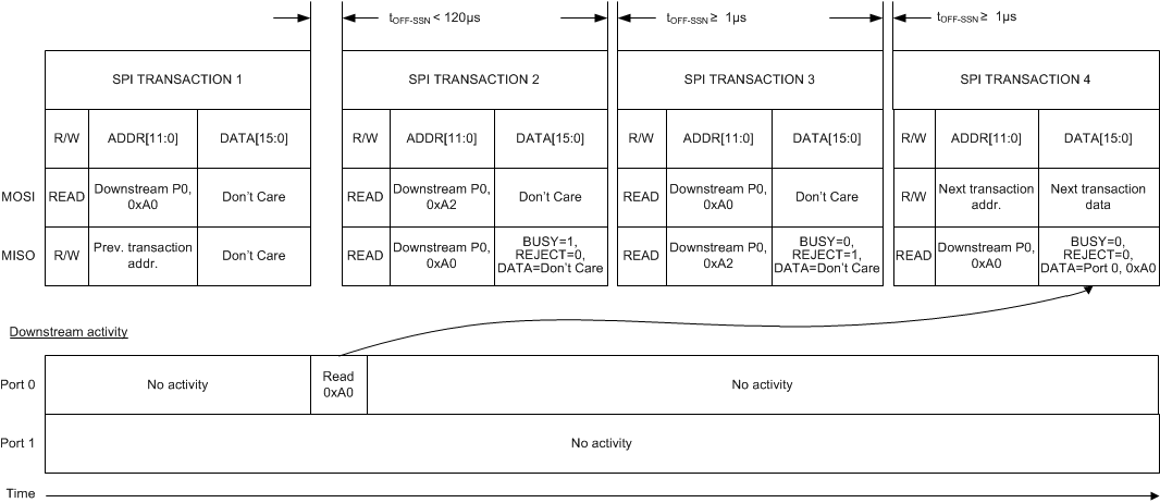
 Figure 7-10 SPI Read Consisting of Two Separate SPI Transactions
For downstream (remote) register reads, where the FPC202 must translate a SPI read into an I2C read transaction with the downstream port, the most significant bit of the data returned on MISO indicates whether the downstream port is busy or not. If the second SPI read transaction is executed prematurely during a downstream (remote) read, the returned data will indicated BUSY = 1. When reading from a downstream port at an address that is not pre-fetched into local FPC202 memory, the time in between the first SPI transaction on a port, where the read is initiated, and the second SPI transaction on the same port, where the data is returned, must be at least 170 µs for a downstream I2C rate of 400 kHz and 620 µs for a downstream I2C rate of 100 kHz. Figure 7-11 shows what happens when this prescribed delay is not followed.
If a back-to-back read transaction is issued to the same downstream port before the FPC202 has completed the first read transaction, then the subsequent transaction will contain status from the second read transaction with REJECT=1, which means that the second transaction was rejected due to the downstream I2C master being busy executing the first read transaction. Figure 7-11 shows what happens when back-to-back reads are issued to the same downstream port without allowing enough time to complete the first read.
 Figure 7-11 Back-to-Back SPI Reads From Same Port