ZHCSBL2C December 2016 – January 2021 HD3SS213
PRODUCTION DATA
5 Pin Configuration and Functions
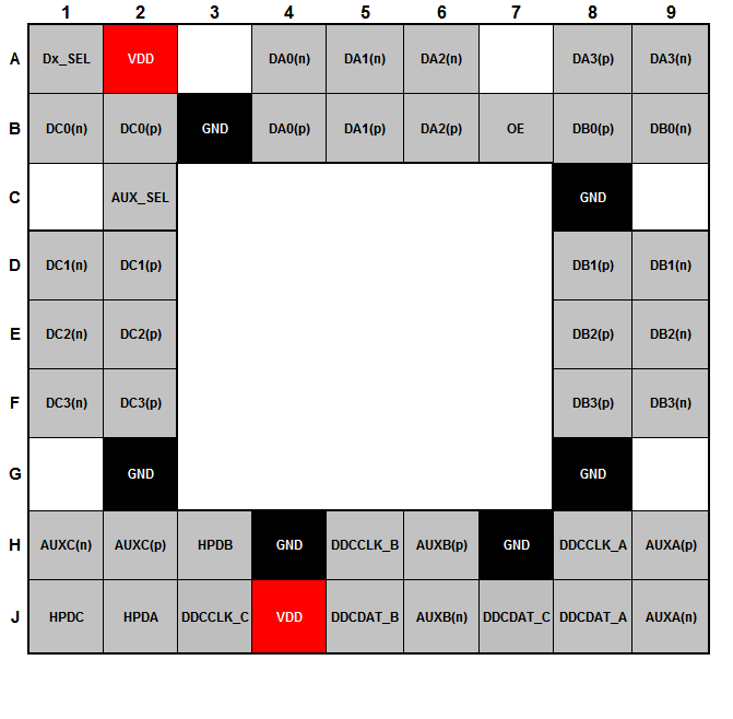
 nFBGA50-Pin ZXH PackageTop View
Table 5-1 Pin Functions
| PIN | TYPE(1) | DESCRIPTION(2) | |
|---|---|---|---|
| NO. | NAME | ||
| H9, J9 |
AUXA(p), AUXA(n) |
I/O | Port A AUX positive signal Port A AUX negative signal |
| H6, J6 |
AUXB(p), AUXB(n) |
I/O | Port B AUX positive signal Port B AUX negative signal |
| H2, H1 |
AUXC(p), AUXC(n) |
I/O | Port C AUX positive signal Port C AUX negative signal |
| C2 | AUX_SEL | I | AUX/DDC selection control pin in conjunction with Dx_SEL Pin |
| NA | CADA/B/C | I/O | Port A/B/C cable activity detect |
| B4, A4 |
DA0(p), DA0(n) |
I/O | Port A, Channel 0, High speed positive signal Port A, Channel 0, High speed negative signal |
| B5, A5 |
DA1(p), DA1(n) |
I/O | Port A, Channel 1, High speed positive signal Port A, Channel 1, High speed negative signal |
| B6, A6 |
DA2(p), DA2(n) |
I/O | Port A, Channel 2, High speed positive signal Port A, Channel 2, High speed negative signal |
| A8, A9 |
DA3(p), DA3(n) |
I/O | Port A, Channel 3, High speed positive signal Port A, Channel 3, High speed negative signal |
| B8, B9 |
DB0(p), DB0(n) |
I/O | Port B, Channel 0, High speed positive signal Port B, Channel 0, High speed negative signal |
| D8, D9 |
DB1(p), DB1(n) |
I/O | Port B, Channel 1, High speed positive signal Port B, Channel 1, High speed negative signal |
| E8, E9 |
DB2(p), DB2(n) |
I/O | Port B, Channel 2, High speed positive signal Port B, Channel 2, High speed negative signal |
| F8, F9 |
DB3(p), DB3(n) |
I/O | Port B, Channel 3, High speed positive signal Port B, Channel 3, High speed negative signal |
| B2, B1 |
DC0(p), DC0(n) |
I/O | Port C, Channel 0, High speed positive signal Port C, Channel 0, High speed negative signal |
| D2, D1 |
DC1(p), DC1(n) |
I/O | Port C, Channel 1, High speed positive signal Port C, Channel 1, High speed negative signal |
| E2, E1 |
DC2(p), DC2(n) |
I/O | Port C, Channel 2, High speed positive signal Port C, Channel 2, High speed negative signal |
| F2, F1 |
DC3(p), DC3(n) |
I/O | Port C, Channel 3, High speed positive signal Port C, Channel 3, High speed negative signal |
| H8, J8 |
DDCCLK_A, DDCDAT_A |
I/O | Port A DDC clock signal Port A DDC data signal |
| H5, J5 |
DDCCLK_B, DDCDAT_B |
I/O | Port B DDC clock signal Port B DDC data signal |
| J3, J7 |
DDCCLK_C, DDCDAT_C |
I/O | Port C DDC clock signal Port C DDC data signal |
| A1 | Dx_SEL | I | High speed port selection control pins |
| B3, C8, G2, G8, H4, H7 |
GND | S | Ground |
| J2 | HPDA | I/O | Port A hot plug detect |
| H3 | HPDB | I/O | Port B hot plug detect |
| J1 | HPDC | I/O | Port C hot plug detect |
| B7 | OE | I | Output enable: OE = VIH: Normal operation OE = VIL: Standby mode |
| A2, J4 |
VDD | S | 3.3-V positive power supply voltage |
(1) I = Input, O = Output, S = Supply
(2) The high speed data ports incorporate 20-kΩ pulldown resistors
that are switched in when a port is not selected and switched out when the port
is selected.