ZHCSE00E may 2014 – december 2020 HD3SS215
PRODUCTION DATA
- 1
- 1 特性
- 2 应用
- 3 说明
- 4 Revision History
- 5 Description (continued)
- 6 Pin Configuration and Functions
-
7 Specifications
- 7.1 Absolute Maximum Ratings #GUID-892340A8-A891-4B90-B8E2-B582AB533890/SLAS9018663 #GUID-892340A8-A891-4B90-B8E2-B582AB533890/SLAS9012713
- 7.2 ESD Ratings
- 7.3 Recommended Operating Conditions
- 7.4 Thermal Information
- 7.5 Electrical Characteristics
- 7.6 Electrical Characteristics, Device Parameters #GUID-222D29AA-746D-4606-8967-F0F2E648EFF8/SLAS9019128
- 7.7 Switching Characteristics
- 7.8 Timing Diagrams
- 8 Detailed Description
- 9 Applications and Implementation
- Power Supply Recommendations
- 10Layout
- 11Device and Documentation Support
- 12Mechanical, Packaging, and Orderable Information
封装选项
机械数据 (封装 | 引脚)
散热焊盘机械数据 (封装 | 引脚)
- RTQ|56
订购信息
10.2 Layout Example
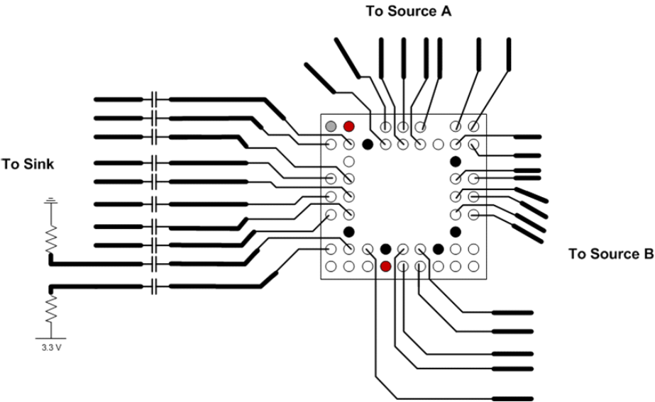
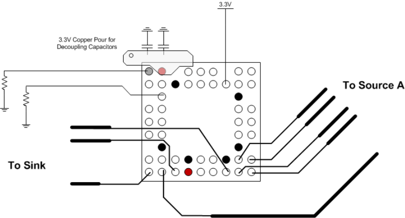
An example layout for the HD3SS215 shows the device implemented on a 4-layer board. The layout figures follow the DisplayPort application schematic above. The top layer layout view shows the signal routing for two sources and one sink. The bottom layer layout view shows the remaining signal routing and a copper pour implemented for the decoupling capacitors.
 Figure 10-1 Top Layer Layout View
 Figure 10-2 Bottom Layer Layout View
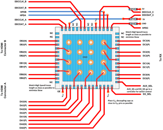
 Figure 10-3 RTQ Layout for 2:1 HDMI Sink Application