ZHCSE00E may 2014 – december 2020 HD3SS215
PRODUCTION DATA
- 1
- 1 特性
- 2 应用
- 3 说明
- 4 Revision History
- 5 Description (continued)
- 6 Pin Configuration and Functions
-
7 Specifications
- 7.1 Absolute Maximum Ratings #GUID-892340A8-A891-4B90-B8E2-B582AB533890/SLAS9018663 #GUID-892340A8-A891-4B90-B8E2-B582AB533890/SLAS9012713
- 7.2 ESD Ratings
- 7.3 Recommended Operating Conditions
- 7.4 Thermal Information
- 7.5 Electrical Characteristics
- 7.6 Electrical Characteristics, Device Parameters #GUID-222D29AA-746D-4606-8967-F0F2E648EFF8/SLAS9019128
- 7.7 Switching Characteristics
- 7.8 Timing Diagrams
- 8 Detailed Description
- 9 Applications and Implementation
- Power Supply Recommendations
- 10Layout
- 11Device and Documentation Support
- 12Mechanical, Packaging, and Orderable Information
封装选项
机械数据 (封装 | 引脚)
散热焊盘机械数据 (封装 | 引脚)
- RTQ|56
订购信息
6 Pin Configuration and Functions
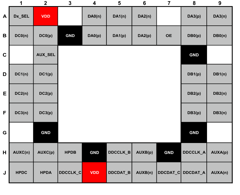
 Figure 6-1 50-Pin
µBGAZXH Package(Top View)
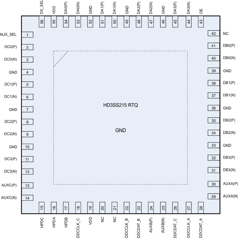
 Figure 6-2 56-Pin QFNRTQ Package(Top View)
Table 6-1 Pin Functions
| PIN | I/O | DESCRIPTION(1) | ||
|---|---|---|---|---|
| NAME | NO. | |||
| ZXH | RTQ | |||
| Dx_SEL | A1 | 56 | 2 Level Control I | High Speed Port Selection Control Pins |
| AUX_SEL | C2 | 1 | 3 Level Control I | AUX/DDC Selection Control Pin in Conjunction with Dx_SEL Pin |
| DA0(p) | B4 | 54 | I/O | Port A, Channel 0, High Speed Positive Signal |
| DA0(n) | A4 | 53 | Port A, Channel 0, High Speed Negative Signal | |
| DA1(p) | B5 | 51 | I/O | Port A, Channel 1, High Speed Positive Signal |
| DA1(n) | A5 | 50 | Port A, Channel 1, High Speed Negative Signal | |
| DA2(p) | B6 | 48 | I/O | Port A, Channel 2, High Speed Positive Signal |
| DA2(n) | A6 | 47 | Port A, Channel 2, High Speed Negative Signal | |
| DA3(p) | A8 | 45 | I/O | Port A, Channel 3, High Speed Positive Signal |
| DA3(n) | A9 | 44 | Port A, Channel 3, High Speed Negative Signal | |
| DB0(p) | B8 | 41 | I/O | Port B, Channel 0, High Speed Positive Signal |
| DB0(n) | B9 | 40 | Port B, Channel 0, High Speed Negative Signal | |
| DB1(p) | D8 | 38 | I/O | Port B, Channel 1, High Speed Positive Signal |
| DB1(n) | D9 | 37 | Port B, Channel 1, High Speed Negative Signal | |
| DB2(p) | E8 | 35 | I/O | Port B, Channel 2, High Speed Positive Signal |
| DB2(n) | E9 | 34 | Port B, Channel 2, High Speed Negative Signal | |
| DB3(p) | F8 | 32 | I/O | Port B, Channel 3, High Speed Positive Signal |
| DB3(n) | F9 | 31 | Port B, Channel 3, High Speed Negative Signal | |
| DC0(p) | B2 | 2 | I/O | Port C, Channel 0, High Speed Positive Signal |
| DC0(n) | B1 | 3 | Port C, Channel 0, High Speed Negative Signal | |
| DC1(p) | D2 | 5 | I/O | Port C, Channel 1, High Speed Positive Signal |
| DC1(n) | D1 | 6 | Port C, Channel 1, High Speed Negative Signal | |
| DC2(p) | E2 | 8 | I/O | Port C, Channel 2, High Speed Positive Signal |
| DC2(n) | E1 | 9 | Port C, Channel 2, High Speed Negative Signal | |
| DC3(p) | F2 | 11 | I/O | Port C, Channel 3, High Speed Positive Signal |
| DC3(n) | F1 | 12 | Port C, Channel 3, High Speed Negative Signal | |
| AUXA(p) | H9 | 30 | I/O | Port A AUX Positive Signal |
| AUXA(n) | J9 | 29 | Port A AUX Negative Signal | |
| AUXB(p) | H6 | 24 | I/O | Port B AUX Positive Signal |
| AUXB(n) | J6 | 25 | Port B AUX Negative Signal | |
| AUXC(p) | H2 | 13 | I/O | Port C AUX Positive Signal |
| AUXC(n) | H1 | 14 | Port C AUX Negative Signal | |
| DDCCLK_A | H8 | 27 | I/O | Port A DDC Clock Signal |
| DDCDAT_A | J8 | 28 | Port A DDC Data Signal | |
| DDCCLK_B | H5 | 22 | I/O | Port B DDC Clock Signal |
| DDCDAT_B | J5 | 23 | Port B DDC Data Signal | |
| DDCCLK_C | J3 | 18 | I/O | Port C DDC Clock Signal |
| DDCDAT_C | J7 | 26 | Port C DDC Data Signal | |
| HPDA/B/C | J2, H3, J1 | 16, 17, 15 | I/O | Port A/B/C Hot Plug Detect |
| OE | B7 | 43 | I | Output Enable: OE = VIH: Normal Operation OE = VIL: Standby Mode |
| VDD | A2, J4 | 19, 55 | Supply | 3.3 V Positive power supply voltage |
| GND | B3, C8, G2, G8 H4, H7 | 4, 7, 10, 33, 36, 39, 46, 49, 52 | Supply | Ground |
| NC | 20, 21, 42 | Not connected | ||
| Thermal Pad | – | – | GND | Supply Ground |
(1) Only the high speed data DAz/DBz ports incorporate 20kΩ pull
down resistors that are switched in when a port is not selected and switched out
when the port is selected.