ZHCSDQ7 May 2015 HD3SS3212
PRODUCTION DATA.
- 1 特性
- 2 应用
- 3 说明
- 4 简化电路原理图
- 5 修订历史记录
- 6 Device Comparison Table
- 7 Pin Configuration and Functions
- 8 Specifications
- 9 Parameter Measurement Information
- 10Detailed Description
- 11Application and Implementation
- 12Power Supply Recommendations
- 13Layout
- 14器件和文档支持
- 15机械、封装和可订购信息
10 Detailed Description
10.1 Overview
The HD3SS3212 is a generic analog differential passive switch that can work for any high-speed interface applications requiring a common mode voltage range of 0 to 2 V and differential signaling with differential amplitude up to 1800 mVpp. It employs adaptive tracking that ensures the channel remains unchanged for the entire common mode voltage range.
Excellent dynamic characteristics of the device allow high-speed switching with minimum attenuation to the signal eye diagram with very little added jitter. It consumes <2 mW of power when operational and has a shutdown mode exercisable by OEn pin resulting <20 µW.
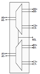
10.2 Functional Block Diagram

10.3 Feature Description
10.3.1 Output Enable and Power Savings
The HD3SS3212 has two power modes, active/normal operating mode and standby/shutdown mode. During standby mode, the device consumes very-little current to save the maximum power. To enter standby mode, the OEn control pin is pulled high through a resistor and must remain high. For active/normal operation, the OEn control pin should be pulled low to GND or dynamically controlled to switch between H or L.
HD3SS3212 consumes <2 mW of power when operational and has a shutdown mode exercisable by the EN pin resulting <20 µW.
10.4 Device Functional Modes
Table 1. Port Select Control Logic(1)
| Port A Channel | Port B or Port C Channel Connected to Port A Channel | |
|---|---|---|
| SEL = L | SEL = H | |
| A0p | B0p | C0p |
| A0n | B0n | C0n |
| A1p | B1p | C1p |
| A1n | B1n | C1n |