ZHCSDQ7 May 2015 HD3SS3212
PRODUCTION DATA.
- 1 特性
- 2 应用
- 3 说明
- 4 简化电路原理图
- 5 修订历史记录
- 6 Device Comparison Table
- 7 Pin Configuration and Functions
- 8 Specifications
- 9 Parameter Measurement Information
- 10Detailed Description
- 11Application and Implementation
- 12Power Supply Recommendations
- 13Layout
- 14器件和文档支持
- 15机械、封装和可订购信息
11 Application and Implementation
NOTE
Information in the following applications sections is not part of the TI component specification, and TI does not warrant its accuracy or completeness. TI’s customers are responsible for determining suitability of components for their purposes. Customers should validate and test their design implementation to confirm system functionality.
11.1 Application Information
The HD3SS3212 is a generic 2-channel high-speed mux/demux type of switch that can be used for routing high-speed signals between two different locations on a circuit board. The HD3SS3212 supports several high-speed data protocols with a differential amplitude of <1800 mVpp and a common mode voltage of <2.0 V, as with USB 3.0 and DisplayPort 1.2. The device’s one select input (SEL) pin can easily be controlled by an available GPIO pin within a system or from a microcontroller.
The HD3SS3212 with its adaptive common mode tracking technology can support applications where the common mode is different between the RX and TX pair. The two USB3.1 Type C connector applications show both a host and device side. The cable between the two connectors swivels the pairs to properly route the signals to the correct pin. The other applications are more generic because different connectors can be used.
Many interfaces require AC coupling between the transmitter and receiver. The 0402 capacitors are the preferred option to provide AC coupling; 0603 size capacitors also work. Avoid the 0805 size capacitors and C-packs. When placing AC coupling capacitors, symmetric placement is best. A capacitor value of 0.1 µF is best, and the value should match for the ±signal pair. The designer should place them along the TX pairs on the system board, which are usually routed on the top layer of the board.
The AC coupling capacitors have several placement options. Because the switch requires a bias voltage, the designer must place the capacitors on one side of the switch. If they are placed on both sides of the switch, a biasing voltage should be provided. Figure 4 shows a few placement options. The coupling capacitors are placed between the switch and endpoint. In this situation, the switch is biased by the system/host controller.
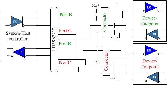 Figure 4. AC Coupling Capacitors between Switch TX and Endpoint TX
In Figure 5, the coupling capacitors are placed on the host transmit pair and endpoint transmit pair. In this situation, the switch on top is biased by the endpoint and the lower switch is biased by the host controller.
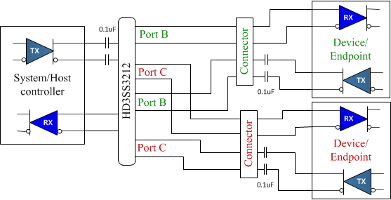 Figure 5. AC Coupling Capacitors on Host TX and Endpoint TX
In the case where the common mode voltage in the system is higher than 2 V, the coupling capacitors are placed on both sides of the switch (shown in Figure 6). A biasing voltage of <2 V is required in this case.
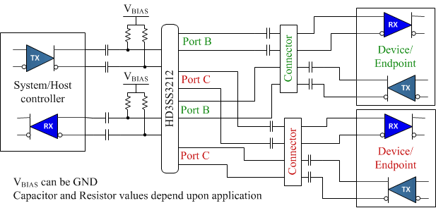 Figure 6. AC Coupling Capacitors on Both Sides of Switch
The HD3SS3212 can be used with the USB Type C connector to support the connector’s flip ability. Figure 7 provides the generic location for the AC coupling capacitors for this application.
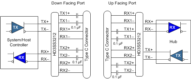 Figure 7. AC Coupling Capacitors for USB Type C
11.2 Typical Applications
11.2.1 Down Facing Port for USB3.1 Type C
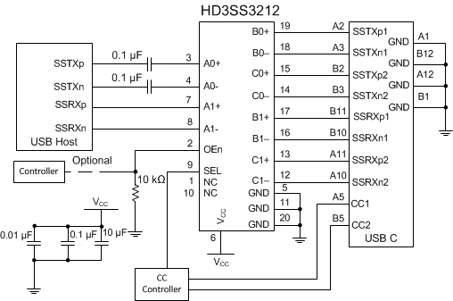 Figure 8. Down Facing Port for USB3.1 Type C Connector
11.2.1.1 Design Requirements
The HD3SS3212 can be designed into many different applications. All the applications have certain requirements for the system to work properly. The HD3SS3212 requires 3.3-V ±10% VCC rail. The OEn pin must be low for device to work otherwise it disables the outputs. This pin can be driven by a processor. The expectation is that one side of the device has AC coupling capacitors. Table 2 provides information on expected values to perform properly.
Table 2. Design Parameters
| DESIGN PARAMETER | VALUE |
|---|---|
| VCC | 3.3 V |
| AXp/n, BXp/n, CXp/n CM input voltage | 0 to 2 V |
| Control/OEn pin max voltage for low | 0.8 V |
| Control/OEn pin min voltage for high | 2.0 V |
| AC coupling capacitor | 100 nF |
| RBIAS (Figure 8) when needed | 1 kΩ |
11.2.1.2 Detailed Design Procedure
The HD3SS3212 is a high-speed passive switch device that can behave as a mux or demux. Because this is a passive switch, signal integrity is important because the device provides no signal conditioning capability. The device can support 2 to 3 inches of board trace and a connector on either end.
To design in the HD3SS3212, the designer needs to understand the following.
- Determine the loss profile between circuits that are to be muxed or demuxed.
- Provide clean impedance and electrical length matched board traces.
- Depending upon the application, determine the best place to put the 100-nF coupling capacitor.
- Provide a control signal for the SEL and OEn pins.
- The thermal pad must be connected to ground.
- See the application schematics on recommended decouple capacitors from VCC pins to ground
11.2.1.3 Application Curves
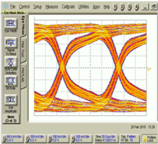 Figure 9. 10 Gbps Source Eye Diagram
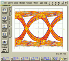 Figure 10. 10 Gbps Output Eye Diagram
11.2.2 Up Facing Port for USB3.1 Type C
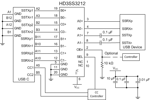 Figure 11. Up Facing Port for USB3.1 USB Type-C Connector
11.2.3 PCIE/SATA/USB
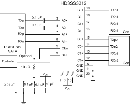 Figure 12. PCIE Motherboard
11.2.4 PCIE/eSATA
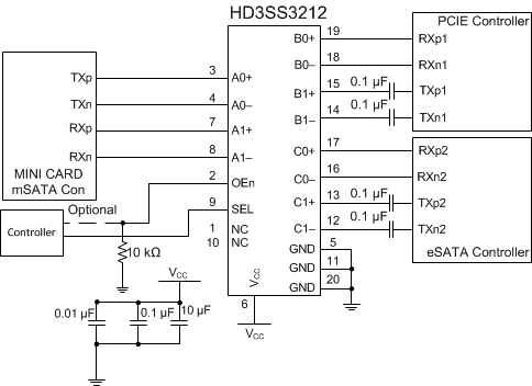 Figure 13. PCIE and eSATA Combo
11.2.5 USB/eSATA
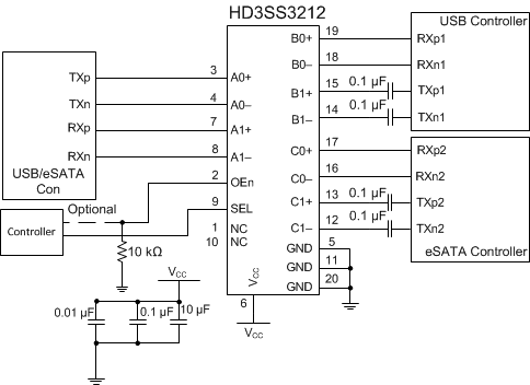 Figure 14. eSATA and USB 3.0 Combo Connector
11.2.6 MIPI Camera Serial Interface
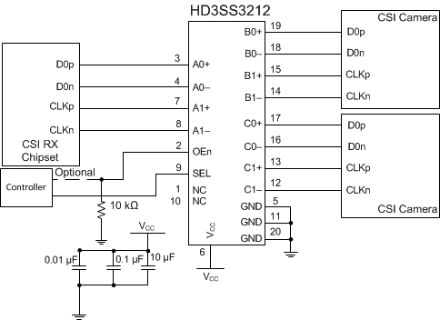 Figure 15. CSI Camera Array