ZHCSBS1A November 2013 – August 2015 HD3SS6126
PRODUCTION DATA.
10 Layout
10.1 Layout Guidelines
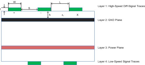
Generally, impedance match becomes critical in such high-speed signal applications to avoid reflection. Each differential-signal pair must have a differential impedance of about 90 Ω ±15% (for PCIe or DP, 100 Ω ±10%) with single-end signal impedance about 50 Ω to ground. Usually, Microstrip is used to accomplish impedance match. Four layers are recommended for a low-EMI PCB design. shows physical geometries of differential traces to form Microstrip. In order to better maintain signal integrity, reference the following:
- Route high-speed differential signals on the top layer with a solid ground layer under them to accomplish controlled impedance, while avoiding vias and stubs which may cause impedance discontinuities. If vias must be used, make sure the space of the vias is as minimal as possible.
- Be sure both the length of differential traces and the length of differential signal pairs are matched in order to reduce intrapair skew and interpair skew separately which also does good to low EMI. TI recommends keeping the space of the traces of the differential signal the same across the entire length of the trace to keep impedance match and reduce EMI.
- Route low-speed, but fast-edged control signals on the bottom layer to minimize the crosstalk of the high-speed signal.
- For other adjacent signal traces on the same layer, make distance L ≥ 3 S to facilitate impedance match.
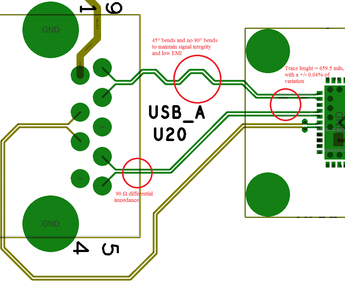
- TI reccommends using 45° bends instead of 90° bends in order to maintain signal integrity and low EMI.
10.2 Layout Examples
 Figure 10. PCB Layers Example
 Figure 11. USB Signals Routing Example