ZHCSBS1A November 2013 – August 2015 HD3SS6126
PRODUCTION DATA.
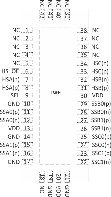
5 Pin Configuration and Functions
RUA Package
42-Pin WQFN
Top View

Pin Functions
| PIN | I/O | DESCRIPTION | |
|---|---|---|---|
| NAME | NO. | ||
| GND | 10, 14, 17, 19, 21 |
Supply | Ground |
| HSA(p) | 8 | I/O | Port A USB 2.0 positive signal |
| HSA(n) | 7 | Port A USB 2.0 negative signal | |
| HSB(p) | 31 | I/O | Port B USB 2.0 positive signal |
| HSB(n) | 32 | Port B USB 2.0 negative signal | |
| HSC(p) | 33 | I/O | Port C USB 2.0 positive signal |
| HSC(n) | 34 | Port C USB 2.0 negative signal | |
| HS_OE | 6 | I (Control) | Output Enable H = Power Down L = Normal Operation |
| NC | 1, 2, 3, 4, 5, 18, 35, 36, 37, 38, 39, 40, 41, 42 |
— | Electrically No Connection |
| SEL | 9 | I (Control) | USB 3.0/2.0 Port Selection Control Pins |
| SSA0(p) | 11 | I/O | Port A, Channel 0, USB 3.0 Positive Signal |
| SSA0(n) | 12 | Port A, Channel 0, USB 3.0 Negative Signal | |
| SSA1(p) | 15 | I/O | Port A, Channel 1, USB 3.0 Positive Signal |
| SSA1(n) | 16 | Port A, Channel 1, USB 3.0 Negative Signal | |
| SSB0(p) | 29 | I/O | Port B, Channel 0, USB 3.0 Positive Signal |
| SSB0(n) | 28 | Port B, Channel 0, USB 3.0 Negative Signal | |
| SSB1(p) | 27 | I/O | Port B, Channel 1, USB 3.0 Positive Signal |
| SSB1(n) | 26 | Port B, Channel 1, USB 3.0 Negative Signal | |
| SSC0(p) | 25 | I/O | Port C, Channel 0, USB 3.0 Positive Signal |
| SSC0(n) | 24 | Port C, Channel 0, USB 3.0 Negative Signal | |
| SSC1(p) | 23 | I/O | Port C, Channel 1, USB 3.0 Positive Signal |
| SSC1(n) | 22 | Port C, Channel 1, USB 3.0 Negative Signal | |
| VDD | 13, 20, 30 | Supply | 3.3-V power supply voltage |