ZHCSCW0A October 2014 – November 2014 HDC1008
PRODUCTION DATA.
- 1 特性
- 2 应用
- 3 说明
- 4 典型应用
- 5 修订历史记录
- 6 Pin Configuration and Functions
- 7 Specifications
- 8 Detailed Description
- 9 Application and Implementation
- 10Power Supply Recommendations
- 11Layout
- 12器件和文档支持
- 13机械封装和可订购信息
11 Layout
11.1 Layout Guidelines
The Relative Humidity sensor element is located on the bottom side of the package. It is positioned between the two rows of bumps.
It is recommended to not route any traces below the sensor element. Moreover, the external components, such as pull-up resistors and bypass capacitors need to be placed next to the 2 rows of bumps or on the bottom side of the PCB in order to guarantee a good air flow.
11.1.1 Surface Mount
Two types of PCB land patterns are used for surface mount packages:
- Non-solder mask defined (NSMD)
- Solder mask defined (SMD)
Pros and cons of NSMD and SMD:
- The NSMD configuration is preferred due to its tighter control of the copper etch process and a reduction in the stress concentration points on the PCB side compared to SMD configuration.
- A copper layer thickness of less than 1 oz. is recommended to achieve higher solder joint stand-off. A 1 oz. (35 micron) or greater copper thickness causes a lower effective solder joint stand-off, which may compromise solder joint reliability.
- For the NSMD pad geometry, the trace width at the connection to the land pad should not exceed 2/3 of the pad diameter.
 Figure 17. Solder Mask
11.1.2 Stencil Printing Process
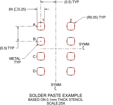
- Use laser cutting followed by electro-polishing for stencil fabrication.
- If possible, offset apertures from land pads to maximize separation and minimize possibility of bridging for DSBGA packages.
- Use Type 3 (25 to 45 micron particle size range) or finer solder paste for printing.
 Figure 18. Solder Paste
11.2 Layout Example
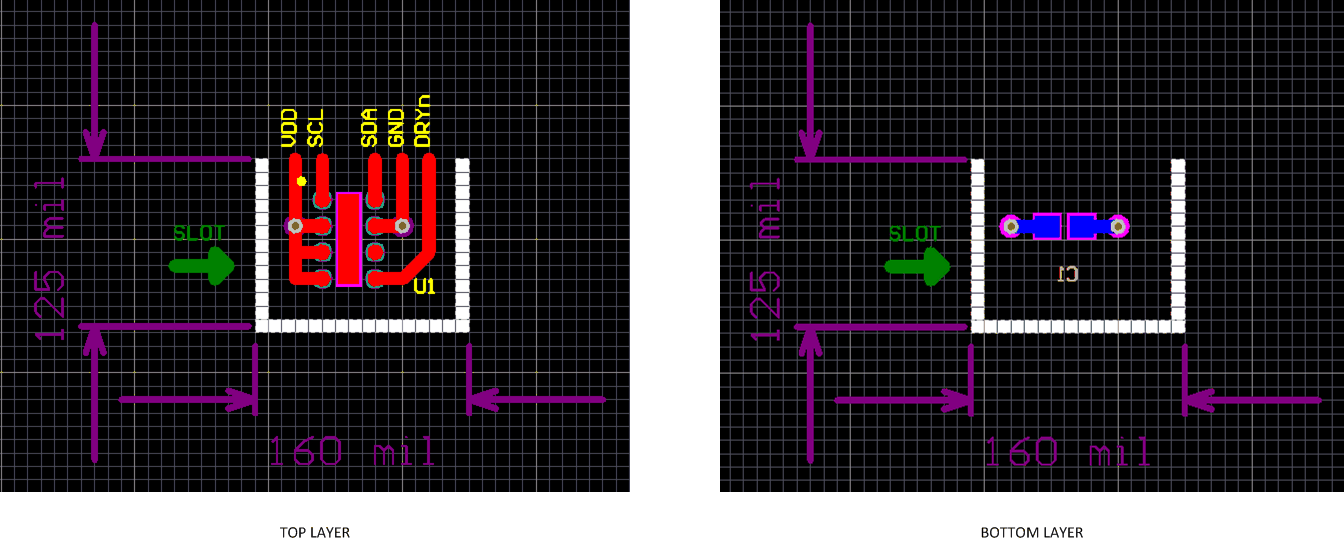
The only component next to the device is the supply bypass capacitor. Since the relative humidity is dependent on the temperature, the HDC1008 should be positioned away from hot points present on the board such as battery, display or micro-controller. Slots around the device can be used to reduce the thermal mass for a quicker response to environmental changes.
 Figure 19. HDC1008 Layout