ZHCSFF0A May   2016  – August 2016 HDC1010

PRODUCTION DATA.  

  1. 特性
  2. 应用
  3. 说明
  4. 典型应用
  5. 修订历史记录
  6. Pin Configuration and Functions
  7. Specifications
    1. 7.1 Absolute Maximum Ratings
    2. 7.2 ESD Ratings
    3. 7.3 Recommended Operating Conditions
    4. 7.4 Thermal Information
    5. 7.5 Electrical Characteristics
    6. 7.6 I2C Interface Electrical Characteristics
    7. 7.7 I2C Interface Timing Requirements
    8. 7.8 Typical Characteristics
  8. Detailed Description
    1. 8.1 Overview
    2. 8.2 Functional Block Diagram
    3. 8.3 Feature Description
      1. 8.3.1 Power Consumption
      2. 8.3.2 Voltage Supply Monitoring
      3. 8.3.3 Heater
    4. 8.4 Device Functional Modes
    5. 8.5 Programming
      1. 8.5.1 I2C Serial Bus Address Configuration
      2. 8.5.2 I2C Interface
        1. 8.5.2.1 Serial Bus Address
        2. 8.5.2.2 Read and Write Operations
        3. 8.5.2.3 Device Measurement Configuration
    6. 8.6 Register Map
      1. 8.6.1 Temperature Register
      2. 8.6.2 Humidity Register
      3. 8.6.3 Configuration Register
      4. 8.6.4 Serial Number Registers
      5. 8.6.5 Manufacturer ID Register
      6. 8.6.6 Device Register ID
  9. Application and Implementation
    1. 9.1 Application Information
    2. 9.2 Typical Application
      1. 9.2.1 Design Requirements
      2. 9.2.2 Detailed Design Procedure
      3. 9.2.3 Application Curve
    3. 9.3 Do's and Don'ts
      1. 9.3.1 Soldering
      2. 9.3.2 Chemical Exposure and Sensor Protection
      3. 9.3.3 High Temperature and Humidity Exposure
  10. 10Power Supply Recommendations
  11. 11Layout
    1. 11.1 Layout Guidelines
      1. 11.1.1 Surface Mount
      2. 11.1.2 Stencil Printing Process
    2. 11.2 Layout Example
  12. 12器件和文档支持
    1. 12.1 文档支持
      1. 12.1.1 相关文档 
    2. 12.2 接收文档更新通知
    3. 12.3 社区资源
    4. 12.4 商标
    5. 12.5 静电放电警告
    6. 12.6 Glossary
  13. 13机械、封装和可订购信息

封装选项

机械数据 (封装 | 引脚)
散热焊盘机械数据 (封装 | 引脚)
订购信息

6 Pin Configuration and Functions

WLCSP (DSBGA)
8 Pin YPA
Top View
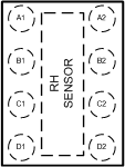
HDC1010 PINOUT.gif

Pin Functions

PIN I/O TYPE(1) DESCRIPTION
NAME NO.
SCL A1 I Serial clock line for I2C, open-drain; requires a pull-up resistor to VDD
VDD B1 P Supply Voltage
ADR0 C1 I Address select pin – hardwired to GND or VDD
ADR1 D1 I Address select pin – hardwired to GND or VDD
SDA A2 I/O Serial data line for I2C, open-drain; requires a pull-up resistor to VDD
GND B2 G Ground
DNC C2 - Do not connect, or, may be connected to GND.
DRDYn D2 O Data ready, active low, open-drain. Requires a pull-up resistor to VDD. If not used tie to GND.
(1) P=Power, G=Ground, I=Input, O=Output