ZHCSTC7A September 2000 – January 2024 INA114
PRODUCTION DATA
- 1
- 1 特性
- 2 应用
- 3 说明
- 4 Pin Configuration and Functions
- 5 Specifications
- 6 Application and Implementation
- 7 Typical Applications
- 8 Device and Documentation Support
- 9 Revision History
- 10Mechanical, Packaging, and Orderable Information
封装选项
请参考 PDF 数据表获取器件具体的封装图。
机械数据 (封装 | 引脚)
- P|8
- DW|16
散热焊盘机械数据 (封装 | 引脚)
订购信息
6.1.7 Output Voltage Sense (SOIC-16 Package Only)
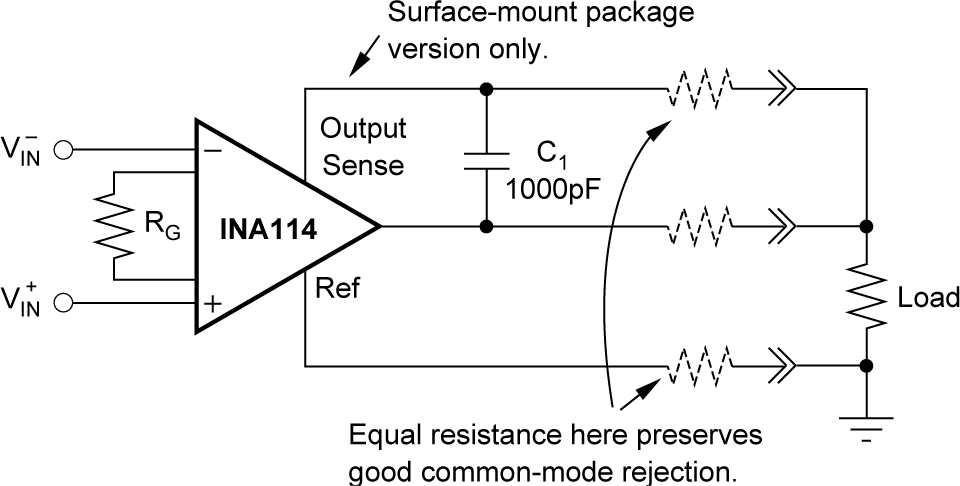
The surface-mount version of the INA114 has a separate output sense feedback connection (pin 12). Pin 12 must be connected to the output terminal (pin 11) for proper operation. (This connection is made internally on the DIP version of the INA114.)
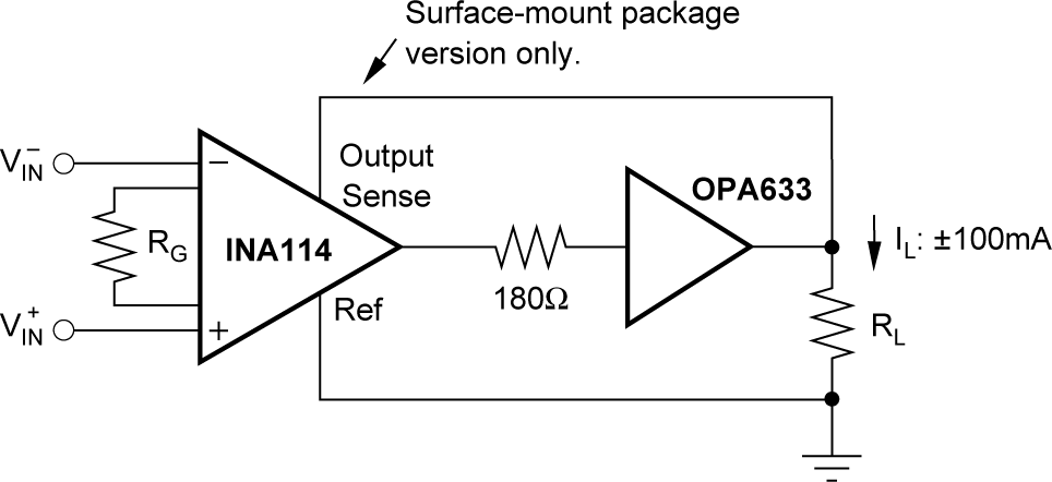
The output sense connection can be used to sense the output voltage directly at the load for best accuracy. Figure 6-5 shows how to drive a load through series interconnection resistance. Remotely located feedback paths can cause instability. This instability can be generally be eliminated with a high-frequency feedback path through C1. Drive heavy loads or long lines by connecting a buffer inside the feedback path (see Figure 6-6).
 Figure 6-5 Remote Load and Ground
Sensing
 Figure 6-6 Buffered Output for Heavy
Loads