ZHCSO32C September 2000 – January 2022 INA126 , INA2126
PRODUCTION DATA
- 1 特性
- 2 应用
- 3 说明
- 4 Revision History
- 5 Pin Configuration and Functions
- 6 Specifications
- 7 Detailed Description
- 8 Application and Implementation
- 9 Power Supply Recommendations
- 10Layout
- 11Device and Documentation Support
- 12Mechanical, Packaging, and Orderable Information
8.2.2.3 Input Bias Current Return
The input impedance of the INAx126 is extremely high at approximately 109 Ω. However, a path must be provided for the input bias current of both inputs. This input bias current is typically –10 nA (current flows out of the input pins). High input impedance means that this input bias current changes very little with varying input voltage.
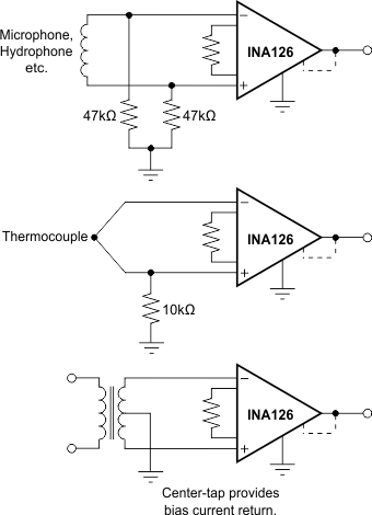
Input circuitry must provide a path for this input bias current for proper operation. Figure 8-3 shows various provisions for an input bias current path. Without a bias current path, the inputs float to a potential that exceeds the common-mode range, and the input amplifiers will saturate.
If the differential source resistance is low, the bias current return path can be connected to one input (see the thermocouple example in Figure 8-3). With higher source impedance, using two equal resistors provides a balanced input with the advantages of lower input offset voltage due to bias current and better high-frequency common-mode rejection.
 Figure 8-3 Providing an Input Common-Mode Current Path