ZHCSHG8F October 1995 – May 2022 INA128 , INA129
PRODUCTION DATA
- 1 特性
- 2 应用
- 3 说明
- 4 Revision History
- 5 Device Comparison Table
- 6 Pin Configuration and Functions
- 7 Specifications
- 8 Detailed Description
- 9 Application and Implementation
- 10Power Supply Recommendations
- 11Layout
- 12Device and Documentation Support
- 13Mechanical, Packaging, and Orderable Information
9.2.2.4 Input Bias Current Return Path
The input impedance of the INA12x is extremely high: approximately 10 GΩ. However, a path must be provided for the input bias current of both inputs. This input bias current is approximately ±2 nA. High input impedance means that this input bias current changes very little with varying input voltage.
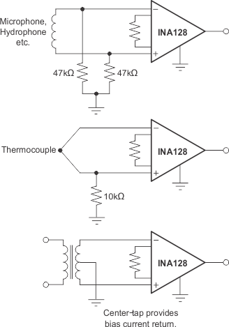
Input circuitry must provide a path for this input bias current for proper operation. Figure 9-3 shows various provisions for an input bias current path. Without a bias current path, the inputs float to a potential that exceeds the common-mode range, and the input amplifiers saturate.
If the differential source resistance is low, the bias current return path can be connected to one input (see the thermocouple example in Figure 9-3). With higher source impedance, use two equal resistors to provide a balanced input, with possible advantages of lower input offset voltage due to bias current, and better high-frequency common-mode rejection.
For more details about why a valid input bias current return path is necessary, see the Importance of Input Bias Current Return Paths in Instrumentation Amplifier Applications application note.
 Figure 9-3 Providing
an Input Common-Mode Current Path