SBOS501F January   2010  – February 2015 INA128-HT , INA129-HT

PRODUCTION DATA.  

  1. Features
  2. Applications
  3. Description
  4. Simplified Schematic
  5. Revision History
  6. Pin Configuration and Functions
  7. Specifications
    1. 7.1 Absolute Maximum Ratings
    2. 7.2 ESD Ratings
    3. 7.3 Recommended Operating Conditions
    4. 7.4 Thermal Information: INA128-HT
    5. 7.5 Electrical Characteristics: INA128-HT
    6. 7.6 Electrical Characteristics: INA129-HT
    7. 7.7 Typical Characteristics
  8. Detailed Description
    1. 8.1 Overview
    2. 8.2 Functional Block Diagram
    3. 8.3 Feature Description
    4. 8.4 Device Functional Modes
      1. 8.4.1 Noise Performance
      2. 8.4.2 Input Common-Mode Range
  9. Application and Implementation
    1. 9.1 Application Information
    2. 9.2 Typical Application
      1. 9.2.1 Design Requirements
      2. 9.2.2 Detailed Design Procedure
        1. 9.2.2.1 Setting the Gain
        2. 9.2.2.2 Dynamic Performance
        3. 9.2.2.3 Offset Trimming
        4. 9.2.2.4 Input Bias Current Return Path
      3. 9.2.3 Application Curves
  10. 10Power Supply Recommendations
    1. 10.1 Low Voltage Operation
  11. 11Layout
    1. 11.1 Layout Guidelines
    2. 11.2 Layout Example
  12. 12Device and Documentation Support
    1. 12.1 Device Support
      1. 12.1.1 Development Support
    2. 12.2 Related Links
    3. 12.3 Trademarks
    4. 12.4 Electrostatic Discharge Caution
    5. 12.5 Glossary
  13. 13Mechanical, Packaging, and Orderable Information

封装选项

机械数据 (封装 | 引脚)
散热焊盘机械数据 (封装 | 引脚)
订购信息

11 Layout

11.1 Layout Guidelines

Place the power-supply bypass capacitor as closely as possible to the supply and ground pins. The recommended value of this bypass capacitor is 0.1 μF to 1 μF. If necessary, additional decoupling capacitance can be added to compensate for noisy or high-impedance power supplies. These decoupling capacitors must be placed between the power supply and INA12x device.

The gain resistor must be placed close to pin 1 and pin 8. This placement limits the layout loop and minimizes any noise coupling into the part.

11.2 Layout Example
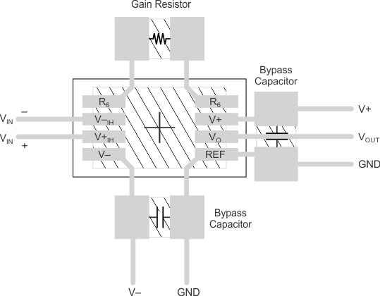
INA128-HT INA129-HT layout_example_bos501.gifFigure 32. Recommended Layout