ZHCSHG8F October   1995  – May 2022 INA128 , INA129

PRODUCTION DATA  

  1. 特性
  2. 应用
  3. 说明
  4. Revision History
  5. Device Comparison Table
  6. Pin Configuration and Functions
  7. Specifications
    1. 7.1 Absolute Maximum Ratings
    2. 7.2 ESD Ratings
    3. 7.3 Recommended Operating Conditions
    4. 7.4 Thermal Information
    5. 7.5 Electrical Characteristics
    6. 7.6 Typical Characteristics
  8. Detailed Description
    1. 8.1 Overview
    2. 8.2 Functional Block Diagram
    3. 8.3 Feature Description
      1. 8.3.1 Noise Performance
    4. 8.4 Device Functional Modes
  9. Application and Implementation
    1. 9.1 Application Information
      1. 9.1.1 Input Common-Mode Range
    2. 9.2 Typical Application
      1. 9.2.1 Design Requirements
      2. 9.2.2 Detailed Design Procedure
        1. 9.2.2.1 Setting the Gain
        2. 9.2.2.2 Dynamic Performance
        3. 9.2.2.3 Offset Trimming
        4. 9.2.2.4 Input Bias Current Return Path
      3. 9.2.3 Application Curves
    3. 9.3 System Examples
  10. 10Power Supply Recommendations
    1. 10.1 Low-Voltage Operation
  11. 11Layout
    1. 11.1 Layout Guidelines
    2. 11.2 Layout Example
  12. 12Device and Documentation Support
    1. 12.1 Device Support
      1. 12.1.1 Development Support
        1. 12.1.1.1 PSpice® for TI
        2. 12.1.1.2 TINA-TI™ Simulation Software (Free Download)
    2. 12.2 Documentation Support
      1. 12.2.1 Related Documentation
    3. 12.3 接收文档更新通知
    4. 12.4 支持资源
    5. 12.5 Trademarks
    6. 12.6 Electrostatic Discharge Caution
    7. 12.7 术语表
  13. 13Mechanical, Packaging, and Orderable Information

封装选项

机械数据 (封装 | 引脚)
散热焊盘机械数据 (封装 | 引脚)
订购信息

Pin Configuration and Functions

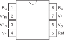
GUID-A95F2DF7-2515-4560-ADDC-03489139938B-low.gifFigure 6-1 D (8-Pin SOIC) and P (8-Pin PDIP) Packages, Top View
Table 6-1 Pin Functions
PIN TYPE DESCRIPTION
NAME NO.
REF 5 Input Reference input. This pin must be driven by low impedance or connected to ground.
RG 1,8 Gain setting pin. For gains greater than 1, place a gain resistor between pin 1 and pin 8.
V– 4 Power Negative supply
V+ 7 Power Positive supply
VIN– 2 Input Negative input
VIN+ 3 Input Positive input
VO 6 Output Output