ZHCSFO0J September 2003 – August 2018 INA138-Q1 , INA168-Q1
PRODUCTION DATA.
- 1 特性
- 2 应用
- 3 说明
- 4 修订历史记录
- 5 Pin Configuration and Functions
- 6 Specifications
- 7 Detailed Description
-
8 Application and Implementation
- 8.1 Application Information
- 8.2 Typical Applications
- 9 Power Supply Recommendations
- 10Layout
- 11器件和文档支持
- 12机械、封装和可订购信息
8.2.3 Offsetting the Output Voltage
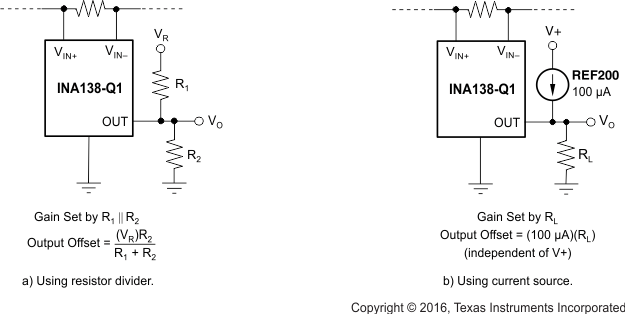
For many applications using only a single power supply, the output voltage may have to be level shifted away from ground when there is no load current flowing in the shunt resistor. Level shifting the output of the INA1x8-Q1 is easily accomplished by one of two simple methods shown in Figure 14. Method (a) on the left-hand side of Figure 14 shows a simple voltage-divider method. This method is useful for applications that require the output of the INA1x8-Q1 to remain centered with respect to the power supply at zero load current through the shunt resistor. Using this method, the gain is determined by the parallel combination of R1 and R2, while the output offset is determined by the voltage divider ratio of R1 and R2, as shown in Figure 14(a). For applications that require a fixed value of output offset independent of the power-supply voltage, use current-source method (b) shown on the right-hand side of Figure 14. With this method, a REF200 constant current source is used to generate a constant output offset. Using this method, the gain is determined by RL, and the offset is determined by the product of the value of the current source and RL.
 Figure 14. Offsetting the Output Voltage