ZHCSFO2E December   1999  – December 2017 INA138 , INA168

PRODUCTION DATA.  

  1. 特性
  2. 应用
  3. 说明
    1.     Device Images
      1.      典型应用电路
  4. 修订历史记录
  5. Pin Configuration and Functions
    1.     Pin Functions
  6. Specifications
    1. 6.1 Absolute Maximum Ratings
    2. 6.2 ESD Ratings
    3. 6.3 Recommended Operating Conditions
    4. 6.4 Thermal Information
    5. 6.5 Electrical Characteristics
    6. 6.6 Typical Characteristics
  7. Detailed Description
    1. 7.1 Overview
    2. 7.2 Functional Block Diagram
    3. 7.3 Feature Description
      1. 7.3.1 Output Voltage Range
      2. 7.3.2 Bandwidth
    4. 7.4 Device Functional Modes
  8. Application and Implementation
    1. 8.1 Application Information
      1. 8.1.1 Operation
    2. 8.2 Typical Applications
      1. 8.2.1 Buffering Output to Drive an ADC
        1. 8.2.1.1 Design Requirements
        2. 8.2.1.2 Detailed Design Procedure
          1. 8.2.1.2.1 Selecting the Shunt Resistor and RL
        3. 8.2.1.3 Application Curve
      2. 8.2.2 Output Filter
        1. 8.2.2.1 Design Requirements
        2. 8.2.2.2 Detailed Design Procedure
        3. 8.2.2.3 Application Curve
      3. 8.2.3 Offsetting the Output Voltage
      4. 8.2.4 Bipolar Current Measurement
      5. 8.2.5 Bipolar Current Measurement Using Differential Input of ADC
      6. 8.2.6 Multiplexed Measurement Using Logic Signal for Power
  9. Power Supply Recommendations
  10. 10Layout
    1. 10.1 Layout Guidelines
    2. 10.2 Layout Example
  11. 11器件和文档支持
    1. 11.1 文档支持
      1. 11.1.1 相关文档
    2. 11.2 相关链接
    3. 11.3 接收文档更新通知
    4. 11.4 社区资源
    5. 11.5 商标
    6. 11.6 静电放电警告
    7. 11.7 Glossary
  12. 12机械、封装和可订购信息

封装选项

机械数据 (封装 | 引脚)
散热焊盘机械数据 (封装 | 引脚)
订购信息

Typical Characteristics

At TA = +25°C, V+ = 5 V, VIN+ = 12 V, and RL = 125 kΩ, unless otherwise noted.
INA138 INA168 graph_1_sbos122.gif
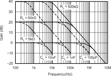
Figure 1. Gain vs Frequency
INA138 INA168 graph_3_sbos122.gif
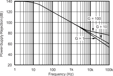
Figure 3. Power-Supply Rejection vs Frequency
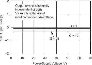
INA138 INA168 graph_5_sbos122.gif
Figure 5. Total Output Error vs Power-Supply Voltage
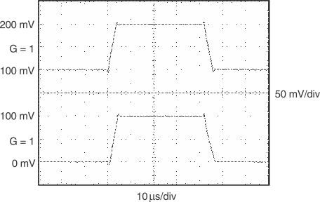
INA138 INA168 g_stepresp01_gls174.gif
Figure 7. Step Response
INA138 INA168 graph_2_sbos122.gif
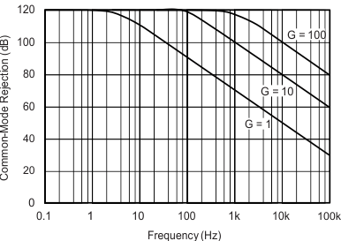
Figure 2. Common-Mode Rejection vs Frequency
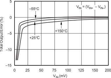
INA138 INA168 graph_4_sbos122.gif
Figure 4. Total Output Error vs VIN
INA138 INA168 graph_6_sbos122.gif
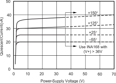
Figure 6. Quiescent Current vs Power-Supply Voltage
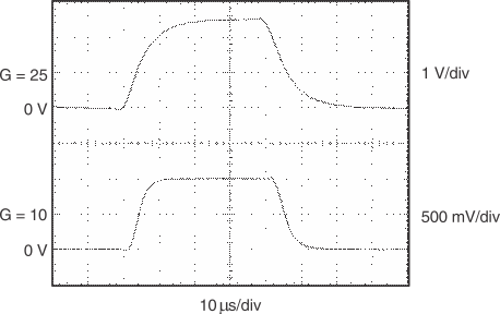
INA138 INA168 g_stepresp02_gls174.gif
Figure 8. Step Response