ZHCSSF8A September   2000  – August 2023 INA141

PRODUCTION DATA  

  1.   1
  2. 1特性
  3. 2应用
  4. 3说明
  5. 4Revision History
  6. 5Pin Configuration and Functions
  7. 6Specifications
    1. 6.1 Absolute Maximum Ratings
    2. 6.2 ESD Ratings
    3. 6.3 Recommended Operating Conditions
    4. 6.4 Thermal Information
    5. 6.5 Electrical Characteristics
    6. 6.6 Typical Characteristics
  8. 7Application and Implementation
    1. 7.1 Application Information
      1. 7.1.1 Setting the Gain
      2. 7.1.2 Dynamic Performance
      3. 7.1.3 Noise Performance
      4. 7.1.4 Offset Trimming
      5. 7.1.5 Input Bias Current Return Path
      6. 7.1.6 Input Common-Mode Range
      7. 7.1.7 Low-Voltage Operation
      8. 7.1.8 Input Protection
  9. 8Device and Documentation Support
    1. 8.1 接收文档更新通知
    2. 8.2 支持资源
    3. 8.3 Trademarks
    4. 8.4 静电放电警告
    5. 8.5 术语表
  10. 9Mechanical, Packaging, and Orderable Information

封装选项

请参考 PDF 数据表获取器件具体的封装图。

机械数据 (封装 | 引脚)
  • D|8
散热焊盘机械数据 (封装 | 引脚)
订购信息

Application Information

Figure 7-1 shows the basic connections required for operation of the INA141. Applications with noisy or high impedance power supplies can require decoupling capacitors close to the device pins as shown.
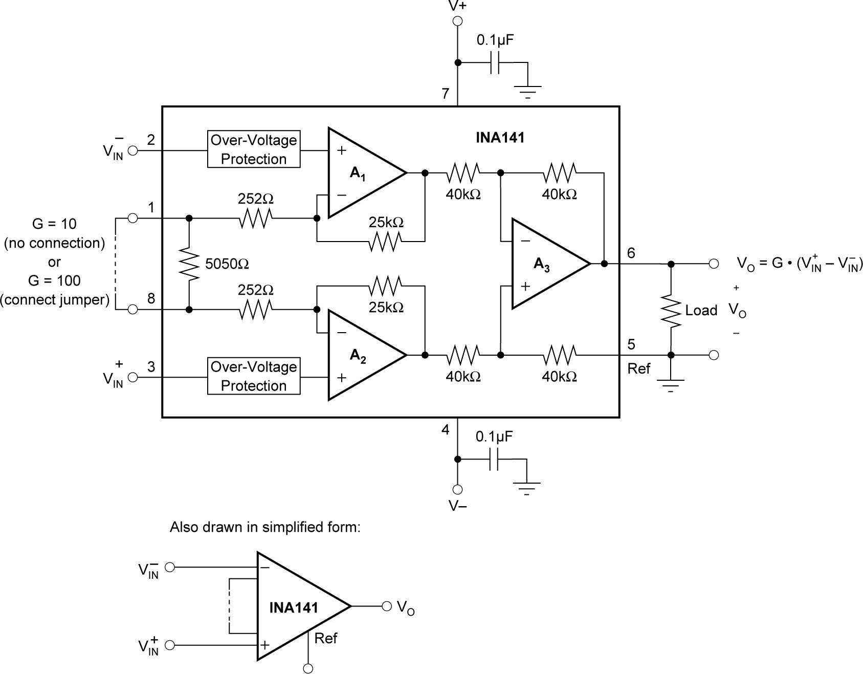
GUID-D858FC97-2213-4158-92DA-A1CF1279A6DB-low.png Figure 7-1 Basic Connections.

The output is referred to the output reference (Ref) pin, which is normally grounded. This connection must be low-impedance to maintain good common-mode rejection. A resistance of 8 Ω in series with the Ref pin causes a typical device to degrade to approximately 80 dB CMR (G = 10 V/V).