ZHCSSF8A September   2000  – August 2023 INA141

PRODUCTION DATA  

  1.   1
  2. 1特性
  3. 2应用
  4. 3说明
  5. 4Revision History
  6. 5Pin Configuration and Functions
  7. 6Specifications
    1. 6.1 Absolute Maximum Ratings
    2. 6.2 ESD Ratings
    3. 6.3 Recommended Operating Conditions
    4. 6.4 Thermal Information
    5. 6.5 Electrical Characteristics
    6. 6.6 Typical Characteristics
  8. 7Application and Implementation
    1. 7.1 Application Information
      1. 7.1.1 Setting the Gain
      2. 7.1.2 Dynamic Performance
      3. 7.1.3 Noise Performance
      4. 7.1.4 Offset Trimming
      5. 7.1.5 Input Bias Current Return Path
      6. 7.1.6 Input Common-Mode Range
      7. 7.1.7 Low-Voltage Operation
      8. 7.1.8 Input Protection
  9. 8Device and Documentation Support
    1. 8.1 接收文档更新通知
    2. 8.2 支持资源
    3. 8.3 Trademarks
    4. 8.4 静电放电警告
    5. 8.5 术语表
  10. 9Mechanical, Packaging, and Orderable Information

封装选项

请参考 PDF 数据表获取器件具体的封装图。

机械数据 (封装 | 引脚)
  • D|8
散热焊盘机械数据 (封装 | 引脚)
订购信息

Pin Configuration and Functions

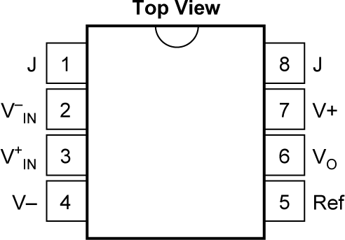
GUID-6BE11181-A970-4A62-986F-1BD986F0E375-low.png Figure 5-1 D Package, 8-Pin SOIC (Top View)
Table 5-1 Pin Functions
PIN TYPE DESCRIPTION
NAME NO.
J 1, 8 Input Gain selection.
G = 10 V/V if not shorted
G = 100 V/V if shorted
A resistance of 0.5 Ω decreases gain by 0.1%.
Ref 5 Input Reference input. This pin must be driven by low impedance
V– 4 Negative supply
V+ 7 Positive supply
VIN 2 Input Negative (inverting) input
V+IN 3 Input Positive (noninverting) input
VO 6 Output Output