ZHCSTR6A September 1999 – November 2023 INA146
PRODUCTION DATA
6.1.5 Input Impedance
The input impedance of the INA146 is determined by the input resistor network and is approximately 100 kΩ. The source impedance at the two input terminals must be nearly equal to maintain good common-mode rejection. A 12-Ω mismatch in impedance between the two inputs causes the typical common-mode rejection to be degraded to approximately 72 dB. Figure 6-7 shows a common application measuring power supply current through a shunt resistor. The source impedance of the shunt resistor, RS, is balanced by an equal compensation resistor, RC.
Source impedances greater than 800 Ω are not recommended, even if the source impedances are perfectly matched. Internal resistors are laser trimmed for accurate ratios, not to absolute values. Adding equal resistors greater than 800 Ω can cause a mismatch in the total resistor ratios, degrading CMR.
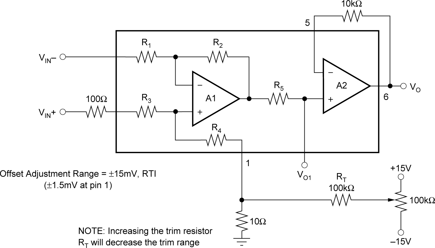 Figure 6-2 Optional Offset Trim Circuit
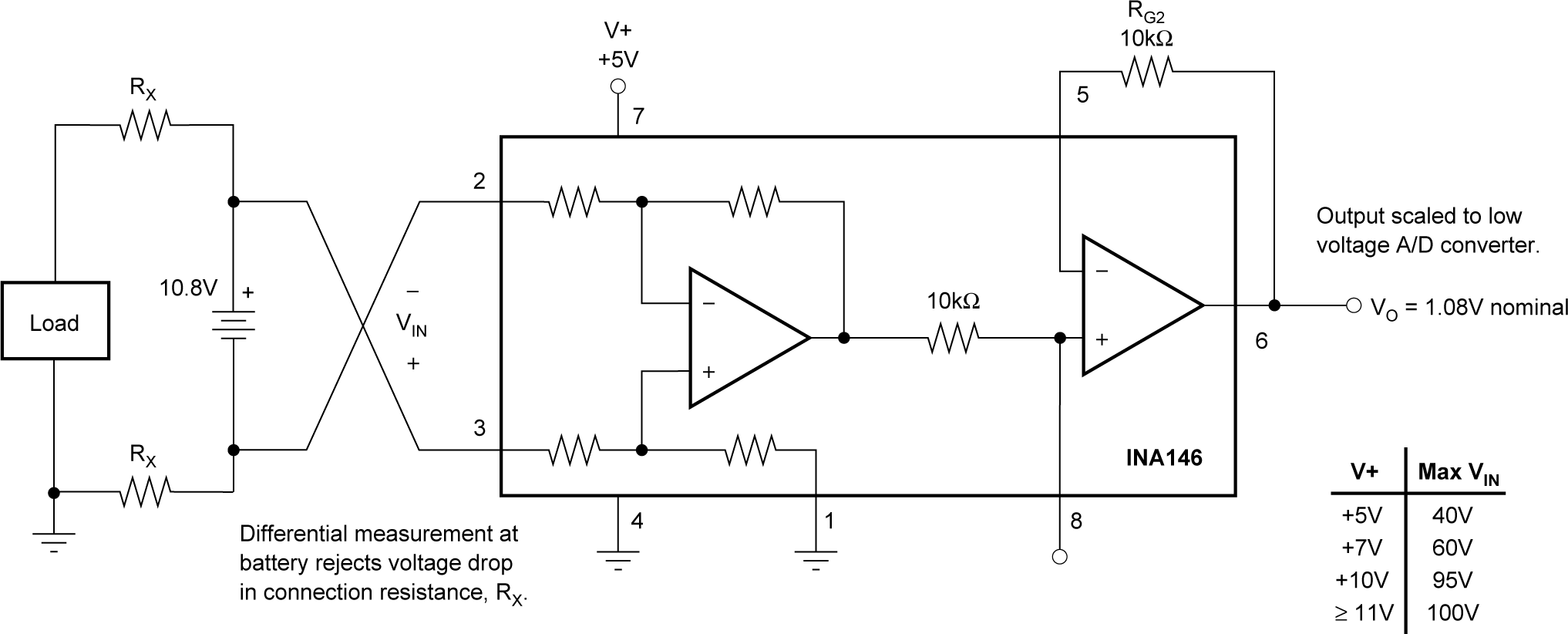 Figure 6-3 Measuring Voltages Greater Than Supply
Voltage
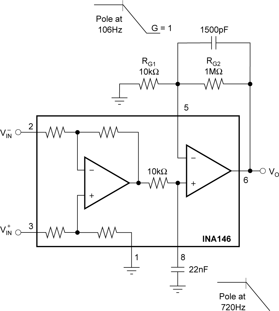 Figure 6-4 Noise Filtering
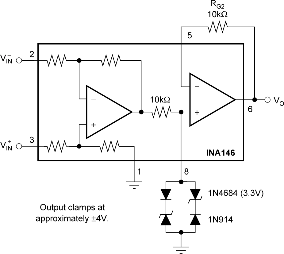 Figure 6-5 Output Clamp
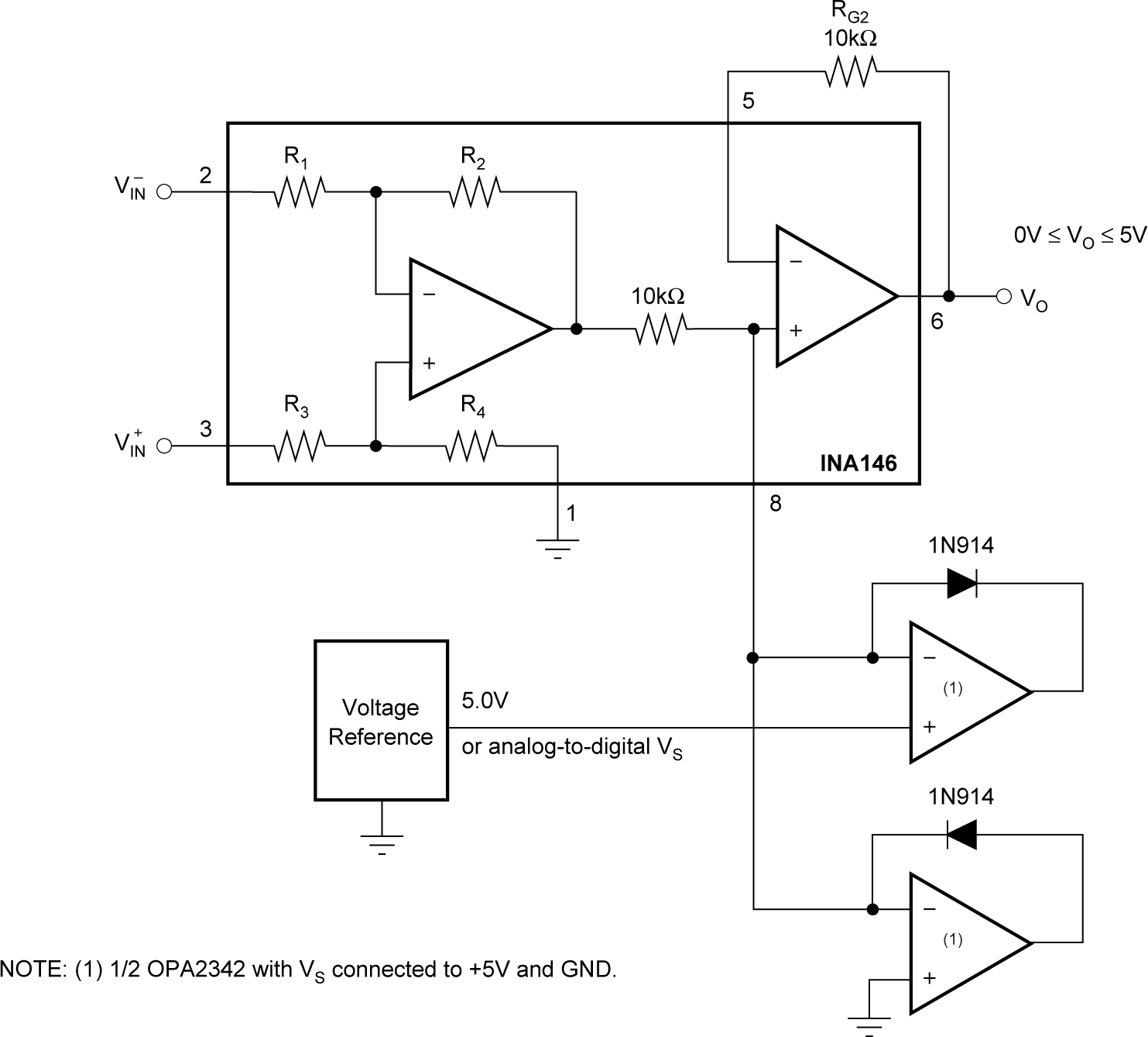 Figure 6-6 Precision Clamp
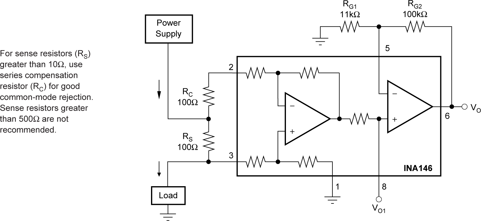 Figure 6-7 Current Monitor, G = 1
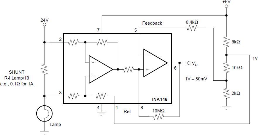 Figure 6-8 Comparator Output With Optional Hysteresis
Application to Sense Lamp Burn-Out
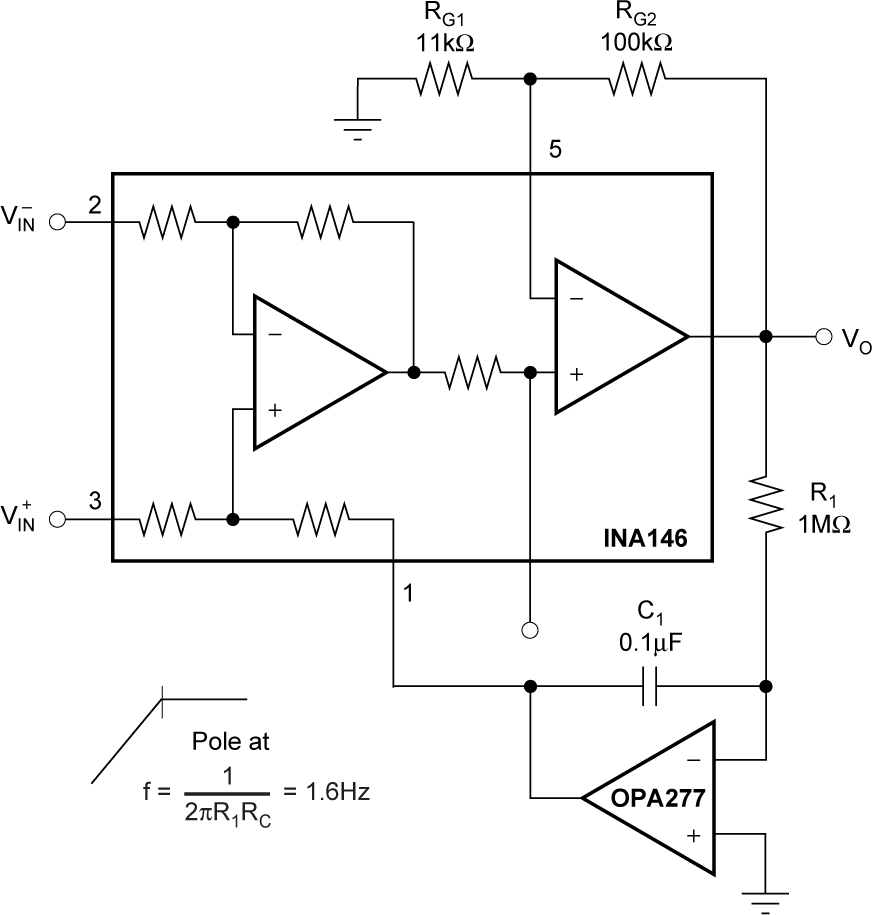 Figure 6-9 AC Coupling (DC Restoration)
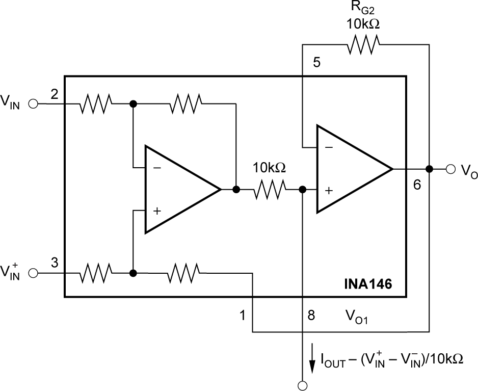 Figure 6-10 Precision Current Source