SBOS472B March 2009 – June 2016 INA148-Q1
PRODUCTION DATA.
- 1 Features
- 2 Applications
- 3 Description
- 4 Revision History
- 5 Pin Configuration and Functions
- 6 Specifications
- 7 Detailed Description
- 8 Application and Implementation
- 9 Power Supply Recommendations
- 10Layout
- 11Device and Documentation Support
- 12Mechanical, Packaging, and Orderable Information
8 Application and Implementation
NOTE
Information in the following applications sections is not part of the TI component specification, and TI does not warrant its accuracy or completeness. TI’s customers are responsible for determining suitability of components for their purposes. Customers should validate and test their design implementation to confirm system functionality.
8.1 Application Information
INA148-Q1 is a unity-gain difference amplifier with a high common-mode input voltage range. It is suitable to be used in many different applications that need bidirectional measurments in a high input common-mode environment.
8.2 Typical Applications
8.2.1 Battery Monitor Circuit
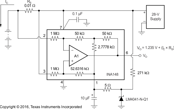 Figure 24. Battery Monitor Circuit Diagram
8.2.1.1 Design Requirements
For this design example, use the parameters listed in Table 1 as the input parameters.
Table 1. Design Parameters
| PARAMETER | EXAMPLE VALUE |
|---|---|
| Battery voltage | 28 V |
| Sense resistor | 0.01 Ω |
| Load current bidirectional | –50 A to 50 A |
| Reference voltage (LM4041-N-Q1) | 1.235 V ± 0.1% |
8.2.1.2 Detailed Design Procedure
This circuit is designed for measuring the high-side current bidirectional in automotive battery monitor such as charging or body control modules with a 28-V battery or similar applications. The voltage difference amplifier REF pin is set at 1.235 V for bidirectional current measurement.
The LM4041-V-Q1 supply current is around 100 µA. It is provided from the 28-V battery through 271-kΩ resistor. The INA148-Q1 has a gain of 1 and output voltage as shown in Equation 3:
The sense resistor value can be changed according to measured current range. TI recommends choosing the right value for minimizing the error and the dissipating power. The measured differential voltage is given as Equation 4 and the dissipated power is given as Equation 5.
8.2.1.3 Application Curves
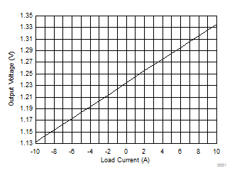 Figure 25. Output Voltage vs Load Current –10 A to 10 A
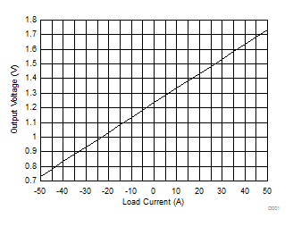 Figure 26. Output Voltage vs Load Current –50 A to 50 A
8.2.2 Quasi-AC-Coupled Differential Amplifier
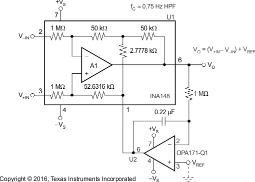 Figure 27. Quasi-AC-Coupled Differential Amplifier Diagram
8.2.2.1 Design Requirements
For this design example, use the parameters listed in Table 2 as the input parameters.
Table 2. Design Parameters
| PARAMETER | EXAMPLE VALUE |
|---|---|
| Common-mode supply voltage (–200 V to 200 V) | 15 V |
| Common-mode supply voltage (–100 V to 750 V) | 5 V |
| U2 | OPA171-Q1 |
| External resistor | 1 MΩ |
| External capacitor | 0.22 µF |
8.2.2.2 Detailed Design Procedure
A quasi-AC coupled differential amplifier can be simply made by adding a general-purpose op amp configured as an integrator externally to the device. Equation 6 shows the output of OPA171-Q1.

where
- ZC is the impedance of the external capacitor
- R is the value of the external resistor
Equation 7 shows the output of INA148-Q1.
Equation 8 is the result of combining the previous two equations.

where
- S = j × 2π × ƒ
The transfer function  has a zero and a pole at
  . Making a gain slope of 20 dB/decade below the cutoff frequncy and flat 0 dB above.
VREF can be set to 0 V in case of dual supply.
8.2.3 Single-Supply Differential Amplifier
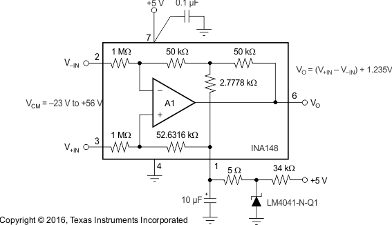 Figure 28. Single-Supply Differential Amplifier Diagram
8.2.3.1 Design Requirements
For this design example, use the parameters listed in Table 3 as the input parameters.
Table 3. Design Parameters
| PARAMETER | EXAMPLE VALUE |
|---|---|
| Common-mode voltage | –23 V to 56 V |
| Load current | Bidirectional |
| Reference voltage (LM4041-N-Q1) | 1.235 V ± 0.1% |
| Supply voltage (INA148-Q1) | 5 V |
8.2.3.2 Detailed Design Procedure
For applications that have –23-V to 56-V common-mode voltage and a single 5-V supply, the common-mode rejection ratio is in the order of 80 dB. The INA148-Q1 is not a rail-to-rail output. An external reference voltage is necessary for bidirectional measurment or low differential output. The external resistor is necessary to provide a 100-µA supply to LM4041-N-Q1.
8.2.4 AC-Coupled Difference Amplifier
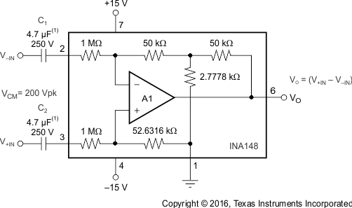
8.2.4.1 Design Requirements
For this design example, use the parameters listed in Table 4 as the input parameters.
Table 4. Design Parameters
| PARAMETER | EXAMPLE VALUE |
|---|---|
| Decoupling capacitors | 4.7 µF, 250 V ± 5% |
| Differential input voltage range | –14 V to 14 V |
8.2.4.2 Detailed Design Procedure
An AC-coupled voltage difference amplifier requires 2 series capacitors. These capacitors must be high quality with tolerance of less than 5% and a rated voltage of 250 V at 200-V common-mode.
8.2.5 50-mV Current-Shunt Amplifier With ±200-V Common-Mode Voltage Range
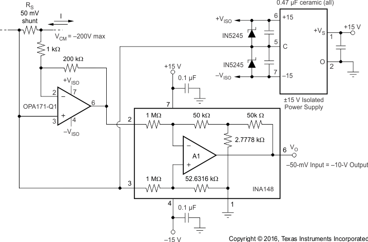 Figure 30. 50-mV Current-Shunt Amplifier With ±200-V Common-Mode Voltage Range Diagram
8.2.5.1 Design Requirements
For this design example, use the parameters listed in Table 5 as the input parameters.
Table 5. Design Parameters
| PARAMETER | EXAMPLE VALUE |
|---|---|
| Common-mode voltage | ±200 V |
| Differential input voltage | –50 mV to 50 mV |
| Gain (OPA171-Q1) | 200 |
| Isolated power supply | ±15 V |
8.2.5.2 Detailed Design Procedure
The OPA171-Q1 gain is 200, set by 1 kΩ and 200 kΩ resistors. The OPA171-Q1 positive input and the INA148‑Q1 are both tied to the isolated power supply common ground. The OPA171-Q1 output is calculated by Equation 9.
where
- VSENSE is the voltage across the shunt resistor
The INA148-Q1 output is calculated by Equation 10.