ZHCSFV5B December 2016 – November 2018 INA1650 , INA1651
PRODUCTION DATA.
- 1 特性
- 2 应用
- 3 说明
- 4 修订历史记录
- 5 Pin Configuration and Functions
- 6 Specifications
- 7 Detailed Description
-
8 Application and Implementation
- 8.1 Application Information
- 8.2
Typical Applications
- 8.2.1 Line Receiver for Differential Audio Signals in a Split-Supply System
- 8.2.2 Differential Line Receiver for Single-Supply Applications
- 8.2.3 Floating Single-Ended Input Line Receiver for Ground Loop Noise Reduction
- 8.2.4 Floating Single-Ended Input Line Receiver With Differential Outputs
- 8.2.5 TRS Audio Interface in Single-Supply Applications
- 8.2.6 Differential Line Driver With Single-Ended Input
- 9 Power Supply Recommendations
- 10Layout
- 11器件和文档支持
- 12机械、封装和可订购信息
7.3.3 Electrical Overstress
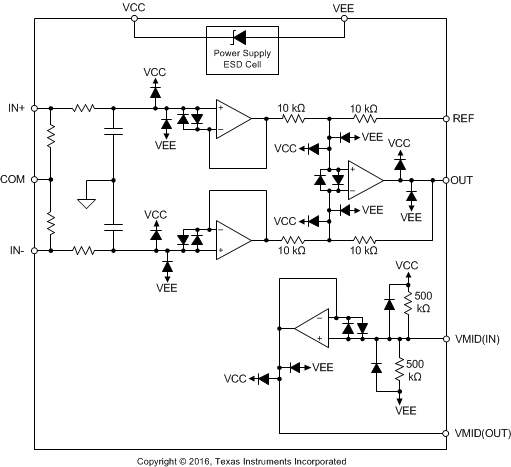
Designers typically ask questions about the capability of an amplifier to withstand electrical overstress. These questions typically focus on the device inputs, but can involve the supply voltage pins or the output pin. Each of these different pin functions have electrical stress limits determined by the voltage breakdown characteristics of the particular semiconductor fabrication process and specific circuits connected to the pin. Additionally, internal ESD protection is built into these circuits to protect them from accidental ESD events both before and during product assembly. A good understanding of basic ESD circuitry and the relevance of circuitry to an electrical overstress event is helpful. Figure 41 illustrates the ESD circuits contained in the INA165x. The ESD protection circuitry involves several current-steering diodes that are connected from the input and output pins and routed back to the internal power-supply lines. This protection circuitry is intended to remain inactive during normal circuit operation. The input pins of the INA165x are protected with internal diodes that are connected to the power-supply rails. These diodes clamp the applied signal to prevent the input circuitry from damage. If the input signal voltage exceeds the power supplies by more than 0.3 V, limit the input signal current to less than 10 mA to protect the internal clamp diodes. A series input resistor can typically limit the current. Some signal sources are inherently current-limited and do not require limiting resistors.
 Figure 41. INA165x Internal ESD Protection Circuitry
(Single Channel and Supply-Divider Shown for Simplicity)