ZHCSFV5B December 2016 – November 2018 INA1650 , INA1651
PRODUCTION DATA.
- 1 特性
- 2 应用
- 3 说明
- 4 修订历史记录
- 5 Pin Configuration and Functions
- 6 Specifications
- 7 Detailed Description
-
8 Application and Implementation
- 8.1 Application Information
- 8.2
Typical Applications
- 8.2.1 Line Receiver for Differential Audio Signals in a Split-Supply System
- 8.2.2 Differential Line Receiver for Single-Supply Applications
- 8.2.3 Floating Single-Ended Input Line Receiver for Ground Loop Noise Reduction
- 8.2.4 Floating Single-Ended Input Line Receiver With Differential Outputs
- 8.2.5 TRS Audio Interface in Single-Supply Applications
- 8.2.6 Differential Line Driver With Single-Ended Input
- 9 Power Supply Recommendations
- 10Layout
- 11器件和文档支持
- 12机械、封装和可订购信息
5 Pin Configuration and Functions
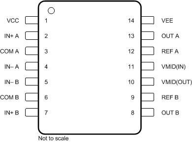
INA1650 PW Package
14-Pin TSSOP
Top View

Pin Functions
| PIN | I/O | DESCRIPTION | |
|---|---|---|---|
| NAME | NO. | ||
| COM A | 3 | I | Input common, channel A |
| COM B | 6 | I | Input common, channel B |
| IN+ A | 2 | I | Noninverting input, channel A |
| IN– A | 4 | I | Inverting input, channel A |
| IN+ B | 7 | I | Noninverting input, channel B |
| IN– B | 5 | I | Inverting input, channel B |
| OUT A | 13 | O | Output, channel A |
| OUT B | 8 | O | Output, channel B |
| REF A | 12 | I | Reference input, channel A. This pin must be driven from a low impedance. |
| REF B | 9 | I | Reference input, channel B. This pin must be driven from a low impedance. |
| VCC | 1 | — | Positive (highest) power supply |
| VEE | 14 | — | Negative (lowest) power supply |
| VMID(IN) | 11 | I | Input node of internal supply divider. Connect a capacitor to this pin to reduce noise from the supply divider circuit. |
| VMID(OUT) | 10 | O | Buffered output of internal supply divider. |
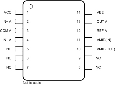
INA1651 PW Package
14-Pin TSSOP
Top View

Pin Functions
| PIN | I/O | DESCRIPTION | |
|---|---|---|---|
| NAME | NO. | ||
| COM A | 3 | I | Input common, channel A |
| IN+ A | 2 | I | Noninverting input, channel A |
| IN– A | 4 | I | Inverting input, channel A |
| NC | 5 | — | No internal connection |
| NC | 6 | — | No internal connection |
| NC | 7 | — | No internal connection |
| NC | 8 | — | No internal connection |
| NC | 9 | — | No internal connection |
| OUT A | 13 | O | Output, channel A |
| REF A | 12 | I | Reference input, channel A. This pin must be driven from a low impedance. |
| VCC | 1 | — | Positive (highest) power supply |
| VEE | 14 | — | Negative (lowest) power supply |
| VMID(IN) | 11 | I | Input node of internal supply divider. Connect a capacitor to this pin to reduce noise from the supply divider circuit. |
| VMID(OUT) | 10 | O | Buffered output of internal supply divider. |