SGLS185F September 2003 – May 2016 INA139-Q1 , INA169-Q1
PRODUCTION DATA.
- 1 Features
- 2 Applications
- 3 Description
- 4 Revision History
- 5 Pin Configuration and Functions
- 6 Specifications
- 7 Detailed Description
-
8 Application and Implementation
- 8.1 Application Information
- 8.2 Typical Applications
- 9 Power Supply Recommendations
- 10Layout
- 11Device and Documentation Support
- 12Mechanical, Packaging, and Orderable Information
7 Detailed Description
7.1 Overview
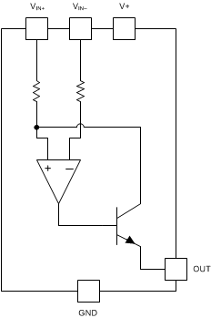
The INA139-Q1 and INA169-Q1 devices (INA1x9-Q1) are comprised of a high voltage, precision operational amplifier, precision thin film resistors trimmed in production to an absolute tolerance and a low noise output transistor. The INA1x9-Q1 are powered from a single power supply, and the input voltages can exceed the power-supply voltage. The INA1x9-Q1 are ideal for measuring small differential voltages, such as those generated across a shunt resistor in the presence of large, common-mode voltages. The Functional Block Diagram illustrates the functional components within both the INA139-Q1 and INA169-Q1 devices.
7.2 Functional Block Diagram

7.3 Feature Description
7.3.1 Output Voltage Range
The output of the INA1x9-Q1 is a current that is converted to a voltage by the load resistor, RL. The output current remains accurate within the compliance voltage range of the output circuitry. The shunt voltage and the input common-mode and power-supply voltages limit the maximum possible output swing. The maximum output voltage (VOUT MAX) compliance is limited by either Equation 1 and Equation 2, whichever is lower:
or
7.3.2 Bandwidth
Measurement bandwidth is affected by the value of the load resistor, RL. High gain produced by high values of RL yields a narrower measurement bandwidth (see the Typical Characteristics section). For the widest possible bandwidth, keep the capacitive load on the output to a minimum. Reduction in bandwidth due to capacitive load is shown in the Typical Characteristics.
If bandwidth limiting (filtering) is desired, add a capacitor can be added to the output (see Figure 12). This capacitor does not cause instability.
7.4 Device Functional Modes
For proper operation, the INA1x9-Q1 must operate within the specified limits. Operating either device outside of their specified power supply voltage range, or their specified common-mode range, results in unexpected behavior, and is not recommended. Additionally, operating the output beyond the specified limits, with respect to power supply voltage and input common-mode voltage, also produces unexpected results. See the Electrical Characteristics for the device specifications.