ZHCSFN5E December 2000 – December 2015 INA139 , INA169
PRODUCTION DATA.
- 1 特性
- 2 应用
- 3 说明
- 4 修订历史记录
- 5 Pin Configuration and Functions
- 6 Specifications
- 7 Detailed Description
-
8 Application and Implementation
- 8.1 Application Information
- 8.2 Typical Applications
- 9 Power Supply Recommendations
- 10Layout
- 11器件和文档支持
- 12机械、封装和可订购信息
7 Detailed Description
7.1 Overview
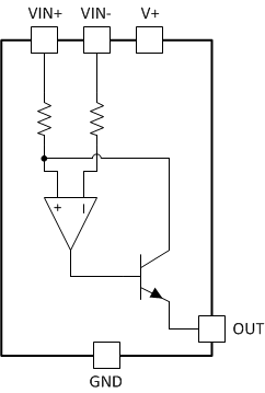
The INA139 and INA169 devices are comprised of a high voltage, precision operational amplifier, precision thin film resistors trimmed in production to an absolute tolerance and a low noise output transistor. The INA139 and INA169 devices can be powered from a single power supply and their input voltages can exceed the power supply voltage. The INA139 and INA169 devices are ideal for measuring small differential voltages, such as those generated across a shunt resistor in the presence of large, common-mode voltages. See Functional Block Diagram, which illustrates the functional components within both the INA139 and INA169 devices.
7.2 Functional Block Diagram

7.3 Feature Description
7.3.1 Output Voltage Range
The output of the INA139 is a current, which is converted to a voltage by the load resistor, RL. The output current remains accurate within the compliance voltage range of the output circuitry. The shunt voltage and the input common-mode and power-supply voltages limit the maximum possible output swing. The maximum output voltage compliance is limited by the lower of Equation 1 and Equation 2.
or
(whichever is lower)
7.3.2 Bandwidth
Measurement bandwidth is affected by the value of the load resistor, RL. High gain produced by high values of RL will yield a narrower measurement bandwidth (see Typical Characteristics). For widest possible bandwidth, keep the capacitive load on the output to a minimum. Reduction in bandwidth due to capacitive load is shown in the Typical Characteristics.
If bandwidth limiting (filtering) is desired, a capacitor can be added to the output (see Figure 12). This will not cause instability.
7.4 Device Functional Modes
For proper operation the INA139 and INA169 devices must operate within their specified limits. Operating either device outside of their specified power supply voltage range or their specified common-mode range will result in unexpected behavior and is not recommended. Additionally operating the output beyond their specified limits with respect to power supply voltage and input common-mode voltage will also produce unexpected results. See Electrical Characteristics for the device specifications.