ZHCSJH3A March 2019 – November 2023 INA185
PRODUCTION DATA
- 1
- 1 特性
- 2 应用
- 3 说明
- 4 Pin Configuration and Functions
- 5 Specifications
- 6 Detailed Description
- 7 Application and Implementation
- 8 Device and Documentation Support
- 9 Revision History
- 10Mechanical, Packaging, and Orderable Information
6.4.2 Unidirectional Mode
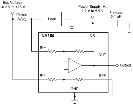
This device is capable of monitoring current flowing in one direction (unidirectional) or in both directions (bidirectional) depending on how the REF pin is configured. The most common case is unidirectional, where the output is set to ground when no current is flowing by connecting the REF pin to ground, as shown in Figure 6-2. When the current flows from the bus supply to the load, the input signal across IN+ to IN– increases, and causes the output voltage at the OUT pin to increase.
 Figure 6-2 Unidirectional Application
The linear range of the output stage is limited by how close the output voltage can approach ground under zero input conditions. In unidirectional applications where measuring very low input currents is desirable, bias the REF pin to a convenient value above 50 mV to get the output into the linear range of the device. To limit common-mode rejection errors, buffer the reference voltage connected to the REF pin.
A less-frequently used output biasing method is to connect the REF pin to the power-supply voltage, VS. This method results in the output voltage saturating at 25 mV less than the supply voltage when no differential input signal is present. This method is similar to the output saturated low condition with no input signal when the REF pin is connected to ground. The output voltage in this configuration only responds to negative currents that develop negative differential input voltage relative to the device IN– pin. Under these conditions, when the differential input signal increases negatively, the output voltage moves downward from the saturated supply voltage. The voltage applied to the REF pin must not exceed VS.