ZHCSE92 September 2015 INA188
UNLESS OTHERWISE NOTED, this document contains PRODUCTION DATA.
6 Specifications
6.1 Absolute Maximum Ratings
over operating free-air temperature range (unless otherwise noted)(1)| MIN | MAX | UNIT | ||
|---|---|---|---|---|
| Voltage | Supply | ±20 | V | |
| 40 (single supply) | ||||
| Current | ±10 | mA | ||
| Analog input range(2) | (V–) – 0.5 | (V+) + 0.5 | V | |
| Output short-circuit(3) | Continuous | |||
| Temperature | Operating range, TA | –55 | 150 | °C |
| Junction, TJ | 150 | |||
| Storage temperature, Tstg | –65 | 150 | ||
(1) Stresses beyond those listed under Absolute Maximum Ratings may cause permanent damage to the device. These are stress ratings only, which do not imply functional operation of the device at these or any other conditions beyond those indicated under Recommended Operating Conditions. Exposure to absolute-maximum-rated conditions for extended periods may affect device reliability.
(2) Input pins are diode-clamped to the power-supply rails. Input signals that can swing more than 0.3 V beyond the supply rails must be current limited to 10 mA or less.
(3) Short-circuit to ground.
6.2 ESD Ratings
| VALUE | UNIT | |||
|---|---|---|---|---|
| V(ESD) | Electrostatic discharge | Human-body model (HBM), per ANSI/ESDA/JEDEC JS-001(1) | ±2500 | V |
| Charged-device model (CDM), per JEDEC specification JESD22-C101(2) | ±1000 | |||
(1) JEDEC document JEP155 states that 500-V HBM allows safe manufacturing with a standard ESD control process.
(2) JEDEC document JEP157 states that 250-V CDM allows safe manufacturing with a standard ESD control process.
6.3 Recommended Operating Conditions
over operating free-air temperature range (unless otherwise noted)| MIN | NOM | MAX | UNIT | ||
|---|---|---|---|---|---|
| VS | Supply voltage | 4 (±2) | 36 (±18) | V | |
| Specified temperature | -40 | 125 | °C | ||
6.4 Thermal Information
| THERMAL METRIC(1) | INA188 | UNIT | ||
|---|---|---|---|---|
| D (SOIC) | DRG (WSON) | |||
| 8 PINS | 8 PINS | |||
| RθJA | Junction-to-ambient thermal resistance | 125 | 145 | °C/W |
| RθJC(top) | Junction-to-case (top) thermal resistance | 80 | 75 | °C/W |
| RθJB | Junction-to-board thermal resistance | 68 | 39 | °C/W |
| ψJT | Junction-to-top characterization parameter | 32 | 14 | °C/W |
| ψJB | Junction-to-board characterization parameter | 68 | 105 | °C/W |
| RθJC(bot) | Junction-to-case (bottom) thermal resistance | N/A | N/A | °C/W |
(1) For more information about traditional and new thermal metrics, see the IC Package Thermal Metrics application report, SPRA953.
6.5 Electrical Characteristics: VS = ±4 V to ±18 V (VS = 8 V to 36 V)
At TA = 25°C, RL = 10 kΩ, VREF = VS / 2, and G = 1, unless otherwise noted.| PARAMETER | TEST CONDITIONS | MIN | TYP | MAX | UNIT | ||
|---|---|---|---|---|---|---|---|
| INPUT(1) | |||||||
| VOSI | Input stage offset voltage | At RTI(2) | ±25 | ±55 | μV | ||
| At RTI, TA = –40°C to +125°C | ±0.08 | ±0.2 | μV/°C | ||||
| VOSO | Output stage offset voltage | At RTI | ±60 | ±170 | μV | ||
| At RTI, TA = –40°C to +125°C | ±0.2 | ±0.35 | μV/°C | ||||
| VOS | Offset voltage | At RTI | ±25 ±60 / G | ±55 ±170 / G | μV | ||
| At RTI, TA = –40°C to +125°C | ±0.2 ±0.35 / G | μV/°C | |||||
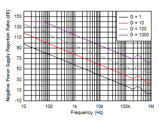
| PSRR | Power-supply rejection ratio | G = 1, VS = 4 V to 36 V, VCM = VS / 2 | ±0.7 | ±2.25 | µV/V | ||
| G = 10, VS = 4 V to 36 V, VCM = VS / 2 | ±0.6 | ||||||
| G = 100, VS = 4 V to 36 V, VCM = VS / 2 | ±0.45 | ||||||
| G = 1000, VS = 4 V to 36 V, VCM = VS / 2 | ±0.3 | ±0.8 | |||||
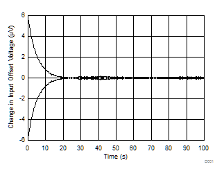
| Long-term stability | 1(3) | µV | |||||
| Turn-on time to specified VOSI | See the Typical Characteristics | ||||||
| zid | Differential input impedance | 100 || 6 | GΩ || pF | ||||
| zic | Common-mode input impedance | 100 || 9.5 | |||||
| VCM | Common-mode voltage range | The input signal common-mode range can be calculated with this tool | (V–) + 0.1 | (V+) – 1.5 | V | ||
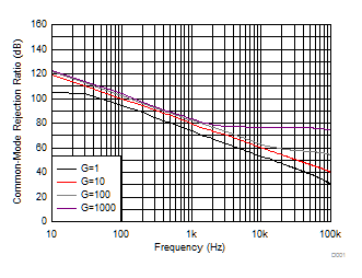
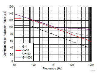
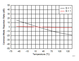
| CMRR | Common-mode rejection ratio | G = 1, at dc to 60 Hz, VCM = (V–) + 1.0 V to (V+) – 2.5 V |
84 | 90 | dB | ||
| G = 10, at dc to 60 Hz, VCM = (V–) + 1.0 V to (V+) – 2.5 V | 104 | 110 | |||||
| G = 100, at dc to 60 Hz, VCM = (V–) + 1.0 V to (V+) – 2.5 V | 118 | 130 | |||||
| G = 1000, at dc to 60 Hz, VCM = (V–) + 1.0 V to (V+) – 2.5 V | 118 | 130 | |||||
| INPUT BIAS CURRENT | |||||||
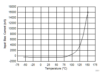
| IIB | Input bias current | ±850 | ±2500 | pA | |||
| TA = –40°C to +125°C | See Figure 10 | pA/°C | |||||
| IOS | Input offset current | ±850 | ±2500 | pA | |||
| TA = –40°C to +125°C | See Figure 11 | pA/°C | |||||
| INPUT VOLTAGE NOISE | |||||||
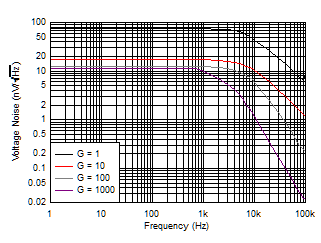
| eNI | Input voltage noise | f = 1 kHz, G = 100, RS = 0 Ω | 12.5 | nV/√Hz | |||
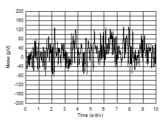
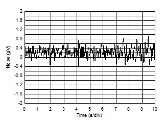
| f = 0.1 Hz to 10 Hz, G = 100, RS = 0 Ω | 0.25 | μVPP | |||||
| eNO | Output voltage noise | f = 1 kHz, G = 100, RS = 0 Ω | 118 | nV/√Hz | |||
| f = 0.1 Hz to 10 Hz, G = 100, RS = 0 Ω | 2.5 | μVPP | |||||
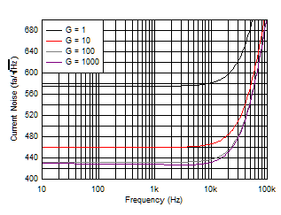
| iN | Input current noise | f = 1 kHz | 440 | fA/√Hz | |||
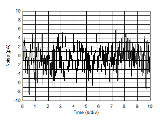
| f = 0.1 Hz to 10 Hz | 10 | pAPP | |||||
| GAIN | |||||||
| G | Gain equation | 1 + (50 kΩ / RG) | V/V | ||||
| Gain range | 1 | 1000 | V/V | ||||
| EG | Gain error | G = 1, (V–) + 0.5 V ≤ VO ≤ (V+) – 1.5 V | ±0.007% | ±0.025% | |||
| G = 10, (V–) + 0.5 V ≤ VO ≤ (V+) – 1.5 V | ±0.05% | ±0.20% | |||||
| G = 100, (V–) + 0.5 V ≤ VO ≤ (V+) – 1.5 V | ±0.06% | ±0.20% | |||||
| G = 1000, (V–) + 0.5 V ≤ VO ≤ (V+) – 1.5 V | ±0.2% | ±0.50% | |||||
| Gain versus temperature | G = 1, TA = –40°C to +125°C | 1 | 5 | ppm/°C | |||
| G > 1(4) , TA = –40°C to +125°C | 15 | 50 | |||||
| Gain nonlinearity | G = 1, VO = –10 V to +10 V | 3 | 8 | ppm | |||
| G > 1, VO = –10 V to +10 V | See Figure 42 to Figure 45 | ||||||
| OUTPUT | |||||||
| Output voltage swing from rail(5) | RL = 10 kΩ(5) | 220 | 250 | mV | |||
| Capacitive load drive | 1 | nF | |||||
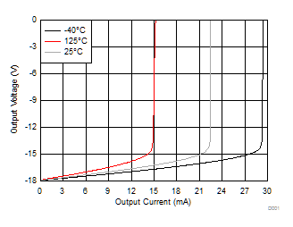
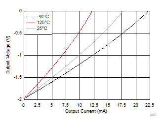
| ISC | Short-circuit current | Continuous to common | ±18 | mA | |||
| FREQUENCY RESPONSE | |||||||
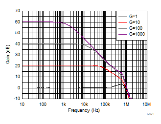
| BW | Bandwidth, –3 dB | G = 1 | 600 | kHz | |||
| G = 10 | 95 | ||||||
| G = 100 | 15 | ||||||
| G = 1000 | 1.5 | ||||||
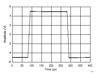
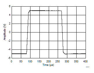
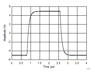
| SR | Slew rate | G = 1, VS = ±18 V, VO = 10-V step | 0.9 | V/μs | |||
| G = 100, VS = ±18 V, VO = 10-V step | 0.17 | ||||||
| tS | Settling time | To 0.1% | G = 1, VS = ±18 V, VSTEP = 10 V | 50 | μs | ||
| G = 100, VS = ±18 V, VSTEP = 10 V | 400 | ||||||
| To 0.01% | G = 1, VS = ±18 V, VSTEP = 10 V | 60 | μs | ||||
| G = 100, VS = ±18 V, VSTEP = 10 V | 500 | ||||||
| Overload recovery | 50% overdrive | 75 | μs | ||||
| REFERENCE INPUT | |||||||
| RIN | Input impedance | 40 | kΩ | ||||
| Voltage range | V– | V+ | V | ||||
| POWER SUPPLY | |||||||
| Voltage range | Single | 4 | 36 | V | |||
| Dual | ±2 | ±18 | |||||
| IQ | Quiescent current | VIN = VS / 2 | 1.4 | 1.6 | mA | ||
| TA = –40°C to +125°C | 1.8 | ||||||
| TEMPERATURE RANGE | |||||||
| Specified temperature range | –40 | 125 | °C | ||||
| Operating temperature range | –55 | 150 | °C | ||||
(1) Total VOS, referred-to-input = (VOSI) + (VOSO / G).
(2) RTI = Referred-to-input.
(3) 300-hour life test at 150°C demonstrated a randomly distributed variation of approximately 1 μV.
(4) Does not include effects of external resistor RG.
6.6 Electrical Characteristics: VS = ±2 V to < ±4 V (VS = 4 V to < 8 V)
At TA = 25°C, RL = 10 kΩ, VREF = VS / 2, and G = 1, unless otherwise noted. Specifications not shown are identical to the Electrical Characteristics table for VS = ±2 V to ±18 V (VS = 8 V to 36 V).| PARAMETER | TEST CONDITIONS | MIN | TYP | MAX | UNIT | ||
|---|---|---|---|---|---|---|---|
| INPUT(1) | |||||||
| VOSI | Input stage offset voltage | At RTI(2) | ±25 | ±55 | μV | ||
| At RTI, TA = –40°C to +125°C | ±0.08 | ±0.2 | μV/°C | ||||
| VOSO | Output stage offset voltage | At RTI | ±60 | ±170 | μV | ||
| At RTI, TA = –40°C to +125°C | ±0.2 | ±0.35 | μV/°C | ||||
| VOS | Offset voltage | At RTI | ±25 ±60 / G | ±55 ±170 / G | μV | ||
| At RTI, TA = –40°C to +125°C | ±0.2 ±0.35 / G | μV/°C | |||||
| Long-term stability | 1(2) | µV | |||||
| Turn-on time to specified VOSI | See the Typical Characteristics | ||||||
| zid | Differential input impedance | 100 || 6 | GΩ || pF | ||||
| zic | Common-mode input impedance | 100 || 9.5 | |||||
| VCM | Common-mode voltage range | VO = 0 V, the input signal common-mode range can be calculated with this tool | (V–) | (V+) – 1.5 | V | ||
| CMRR | Common-mode rejection ratio | G = 1, at dc to 60 Hz, VCM = (V–) + 1.0 V to (V+) – 2.5 V |
80 | 90 | dB | ||
| G = 10, at dc to 60 Hz, VCM = (V–) + 1.0 V to (V+) – 2.5 V |
94 | 110 | |||||
| G = 100, at dc to 60 Hz, VCM = (V–) + 1.0 V to (V+) – 2.5 V | 102 | 120 | |||||
| G = 1000, at dc to 60 Hz, VCM = (V–) + 1.0 V to (V+) – 2.5 V | 102 | 120 | |||||
| INPUT BIAS CURRENT | |||||||
| IIB | Input bias current | ±850 | ±2500 | pA | |||
| TA = –40°C to +125°C | See Figure 10 | pA/°C | |||||
| IOS | Input offset current | ±850 | ±2500 | pA | |||
| TA = –40°C to +125°C | See Figure 11 | pA/°C | |||||
| INPUT VOLTAGE NOISE | |||||||
| eNI | Input voltage noise | f = 1 kHz, G = 100, RS = 0 Ω | 12.5 | nV/√Hz | |||
| f = 0.1 Hz to 10 Hz, G = 100, RS = 0 Ω | 0.25 | μVPP | |||||
| eNO | Output voltage noise | f = 1 kHz, G = 100, RS = 0 Ω | 118 | nV/√Hz | |||
| f = 0.1 Hz to 10 Hz, G = 100, RS = 0 Ω | 2.5 | μVPP | |||||
| iN | Input current noise | f = 1 kHz | 430 | fA/√Hz | |||
| f = 0.1 Hz to 10 Hz | 10 | pAPP | |||||
| GAIN | |||||||
| G | Gain equation | 1 + (50 kΩ / RG) | V/V | ||||
| Gain range | 1 | 1000 | V/V | ||||
| EG | Gain error | G = 1, (V–) + 0.5 V ≤ VO ≤ (V+) – 1.5 V | ±0.007% | ±0.05% | |||
| G = 10, (V–) + 0.5 V ≤ VO ≤ (V+) – 1.5 V | ±0.07% | ±0.2% | |||||
| G = 100, (V–) + 0.5 V ≤ VO ≤ (V+) – 1.5 V | ±0.07% | ±0.2% | |||||
| G = 1000, (V–) + 0.5 V ≤ VO ≤ (V+) – 1.5 V | ±0.25% | ±0.5% | |||||
| Gain versus temperature | G = 1, TA = –40°C to +125°C | 1 | 5 | ppm/°C | |||
| G > 1(3), TA = –40°C to +125°C | 15 | 50 | |||||
| Gain nonlinearity | G = 1, VO = (V–) + 0.5 V ≤ VO ≤ (V+) – 1.5 V | 3 | 8 | ppm | |||
| OUTPUT | |||||||
| Output voltage swing from rail(5) | RL = 10 kΩ | 220 | 250 | mV | |||
| Capacitive load drive | 1 | nF | |||||
| ISC | Short-circuit current | Continuous to common | ±18 | mA | |||
| FREQUENCY RESPONSE | |||||||
| BW | Bandwidth, –3 dB | G = 1 | 600 | kHz | |||
| G = 10 | 95 | ||||||
| G = 100 | 15 | ||||||
| G = 1000 | 1.5 | ||||||
| SR | Slew rate | G = 1, VS = 5 V, VO = 4-V step | 0.9 | V/μs | |||
| G = 100, VS = 5 V, VO = 4-V step | 0.17 | ||||||
| tS | Settling time | To 0.1% | G = 1, VS = 5 V, VSTEP = 4 V | 50 | μs | ||
| G = 100, VS = 5 V, VSTEP = 4 V | 400 | ||||||
| To 0.01% | G = 1, VS = 5 V, VSTEP = 4 V | 60 | μs | ||||
| G = 100, VS = 5 V, VSTEP = 4 V | 500 | ||||||
| Overload recovery | 50% overdrive | 75 | μs | ||||
| REFERENCE INPUT | |||||||
| RIN | Input impedance | 40 | kΩ | ||||
| Voltage range | V– | V+ | V | ||||
| POWER SUPPLY | |||||||
| Voltage range | Single | 4 | 36 | V | |||
| Dual | ±2 | ±18 | |||||
| IQ | Quiescent current | VIN = VS / 2 | 1.4 | 1.6 | mA | ||
| TA = –40°C to +125°C | 1.8 | ||||||
| TEMPERATURE RANGE | |||||||
| Specified temperature range | –40 | 125 | °C | ||||
| Operating temperature range | –55 | 150 | °C | ||||
(1) Total VOS, referred-to-input = (VOSI) + (VOSO / G).
(2) 300-hour life test at 150°C demonstrated randomly distributed variation of approximately 1 μV.
(3) Does not include effects of external resistor RG.
6.7 Typical Characteristics
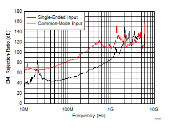
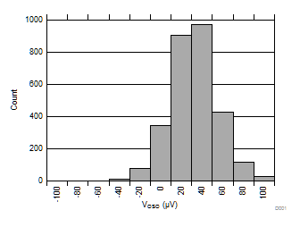
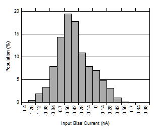
At TA = 25°C, VS = ±15 V, RL = 10 kΩ, VREF = midsupply, and G = 1, unless otherwise noted.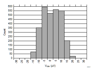
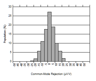
| G = 1 |
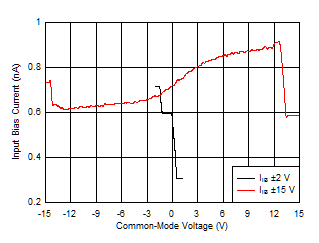
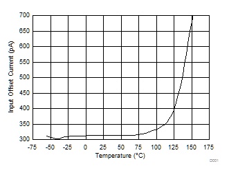
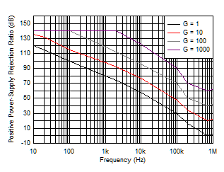
| At RTI |
| At RTI |
| At RTI, 1-kΩ Source Imbalance |
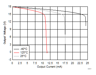
| VS = ±18 V |
Output Current
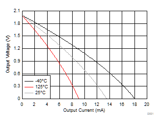
| VS = ±2 V |
Output Current
| G = 1000 |
| RL = 10 kΩ, CL = 100 pF, G = 1 |
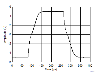
| RL = 10 kΩ, CL = 100 pF, G = 100 |
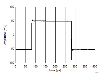
| RL = 10 kΩ, CL = 100 pF, G = 1 |
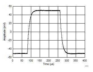
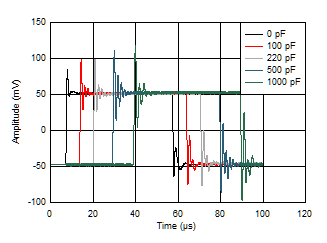
| RL = 10 kΩ, CL = 100 pF, G = 100 |
| G = 1 |
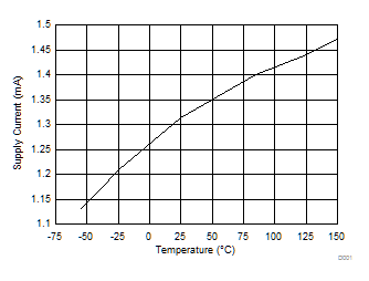
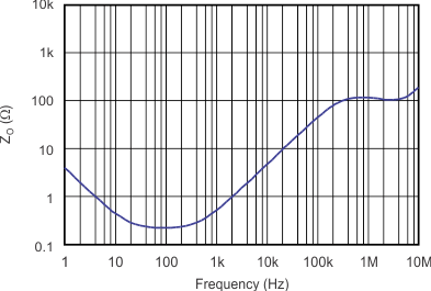
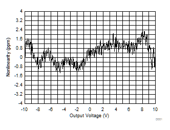
| G = 10 |
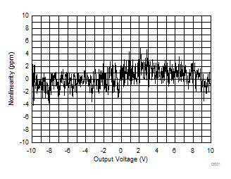
| G = 1000 |
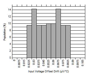
| –40°C to +125°C |
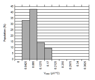
| –40°C to +125°C |
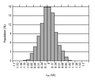
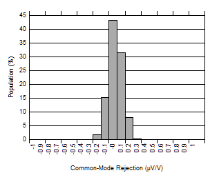
| G = 100 |
| At RTI |
| VS = ±18 V |
Output Current
| VS = ±2 V |
Output Current
| G = 1 |
| RL = 10 kΩ, CL = 100 pF, G = 10 |
| RL = 10 kΩ, CL = 100 pF, G = 1000 |
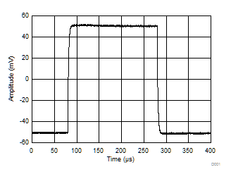
| RL = 10 kΩ, CL = 100 pF, G = 10 |
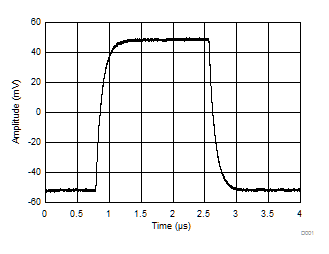
| RL = 10 kΩ, CL = 100 pF, G = 1000 |
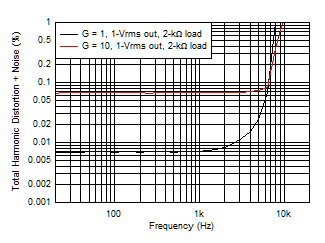
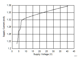
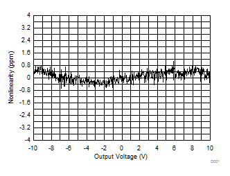
| G = 1 |
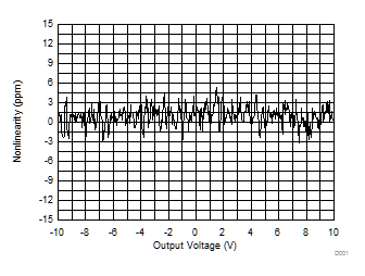
| G = 100 |
