at TA = 25°C, VS = 1.8 V,
VIN+ = 12 V, VREF = VS / 2, VENABLE =
VS(DDF), and for all gain options (unless otherwise
noted)
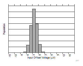
 Figure 6-1 Input Offset Voltage Production Distribution
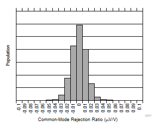
 Figure 6-3 Common-Mode Rejection Production Distribution
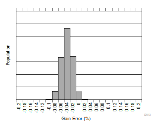
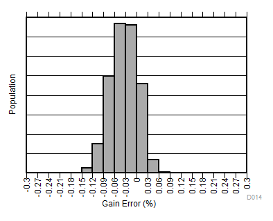
 Figure 6-5 Gain Error Production Distribution
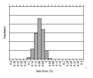
 Figure 6-7 Gain
Error Production Distribution
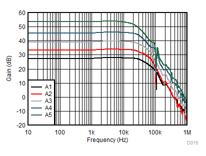
 Figure 6-9 Gain vs. Frequency
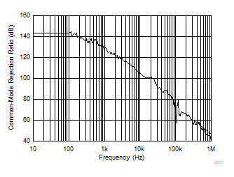
 Figure 6-11 Common-Mode Rejection Ratio vs. Frequency
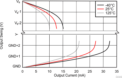
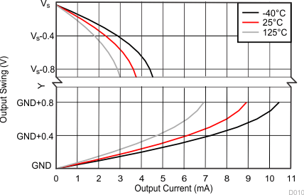
 Figure 6-13 Output Voltage Swing vs. Output Current
 Figure 6-15 Input
Bias Current vs. Common-Mode Voltage (Shutdown)
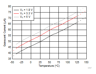
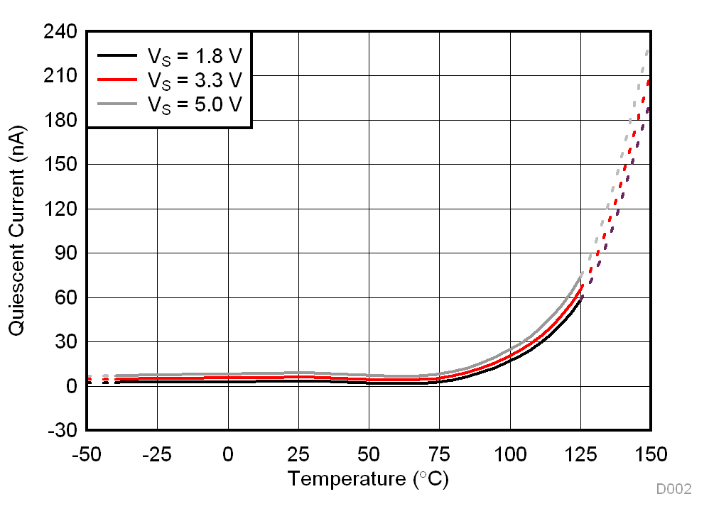
 Figure 6-17 Quiescent Current vs. Temperature (Enabled)
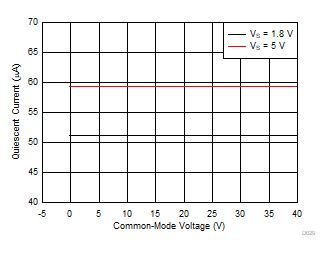
 Figure 6-19 Quiescent Current vs. Common Mode Voltage
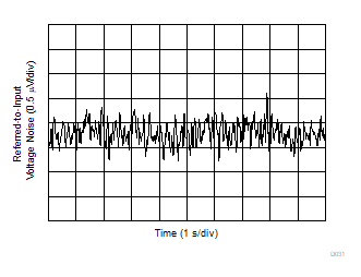
 Figure 6-21 0.1-Hz to 10-Hz Voltage Noise (Referred-To-Input)
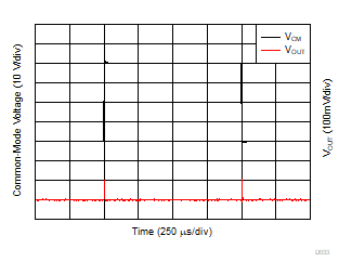
 Figure 6-23 Common-Mode Voltage Transient Response
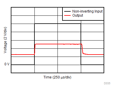
 Figure 6-25 Noninverting Differential Input Overload
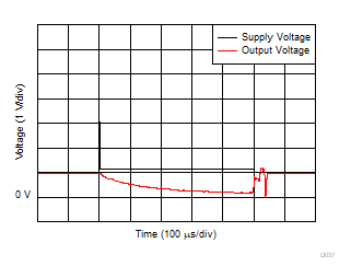
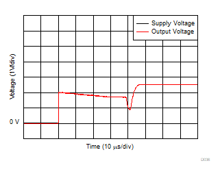
 Figure 6-27 Brownout Recovery
| VS = 5.0 V, VREF = 2.5 V, A1 devices |

| VS = 5.0 V, VENABLE = 0 V,
VREF = 2.5 V |
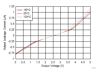
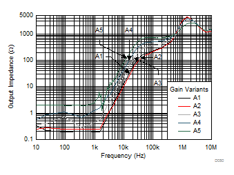
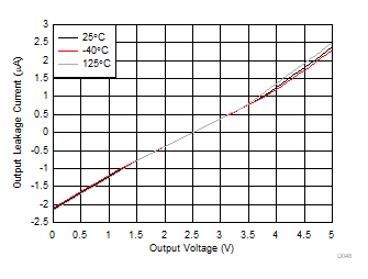
Figure 6-31 Output Leakage vs. Output Voltage (A1, A2, and A3 Devices) Figure 6-33 Output Impedance vs. Frequency
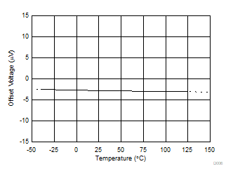
 Figure 6-2 Offset Voltage vs. Temperature
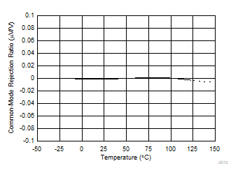
 Figure 6-4 Common-Mode Rejection Ratio vs. Temperature
 Figure 6-6 Gain Error Production Distribution
 Figure 6-8 Gain
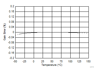
Error vs. Temperature
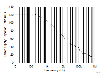
 Figure 6-10 Power-Supply Rejection Ratio vs. Frequency
 Figure 6-12 Output Voltage Swing vs. Output Current
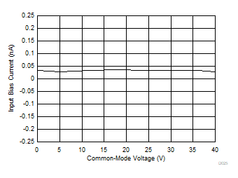
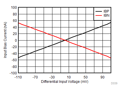
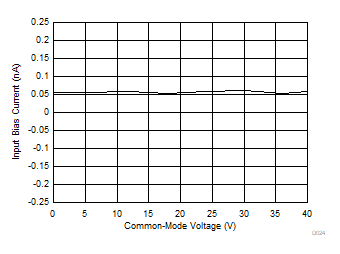
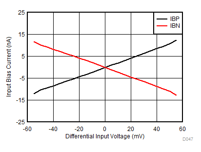
 Figure 6-14 Input
Bias Current vs. Common-Mode Voltage
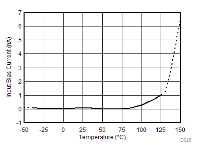
 Figure 6-16 Input
Bias Current vs. Temperature
 Figure 6-18 Quiescent Current vs. Temperature (Disabled)
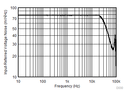
 Figure 6-20 Input-Referred Voltage Noise vs. Frequency
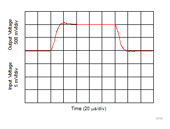
 Figure 6-22 Step Response (10-mVPP Input Step)
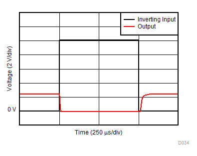
 Figure 6-24 Inverting Differential Input Overload
 Figure 6-26 Start-Up Response
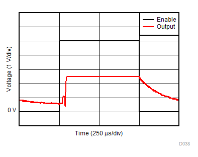
 Figure 6-28 Enable and Disable Response
| VS = 5.0 V, VREF = 2.5 V, A2, A3, A4, A5 devices |

| VS = 5.0 V, VENABLE = 0 V,
VREF = 2.5 V |
Figure 6-32 Output Leakage vs. Output Voltage (A4 and A5 Devices)