ZHCSJE3C february   2019  – august 2021 INA191 , INA2191

PRODUCTION DATA  

  1.   1
  2. 特性
  3. 应用
  4. 说明
  5. Revision History
  6. Pin Configuration and Functions
  7. Specifications
    1. 6.1 Absolute Maximum Ratings
    2. 6.2 ESD Ratings
    3. 6.3 Recommended Operating Conditions
    4. 6.4 Thermal Information
    5. 6.5 Electrical Characteristics
    6. 6.6 Typical Characteristics
  8. Detailed Description
    1. 7.1 Overview
    2. 7.2 Functional Block Diagram
    3. 7.3 Feature Description
      1. 7.3.1 Precision Current Measurement
      2. 7.3.2 Low Input Bias Current
      3. 7.3.3 Low Quiescent Current With Output Enable
      4. 7.3.4 Bidirectional Current Monitoring (INA2191 Only)
      5. 7.3.5 High-Side and Low-Side Current Sensing
      6. 7.3.6 High Common-Mode Rejection
      7. 7.3.7 Rail-to-Rail Output Swing
    4. 7.4 Device Functional Modes
      1. 7.4.1 Normal Operation
      2. 7.4.2 Unidirectional Mode
      3. 7.4.3 Bidirectional Mode (INA2191 Only)
      4. 7.4.4 Input Differential Overload
      5. 7.4.5 Shutdown
  9. Application and Implementation
    1. 8.1 Application Information
      1. 8.1.1 Basic Connections
      2. 8.1.2 RSENSE and Device Gain Selection
      3. 8.1.3 Signal Conditioning
      4. 8.1.4 Common-Mode Voltage Transients
    2. 8.2 Typical Application
      1. 8.2.1 Microamp Current Measurement
        1. 8.2.1.1 Design Requirements
        2. 8.2.1.2 Detailed Design Procedure
        3. 8.2.1.3 Application Curve
  10. Power Supply Recommendations
  11. 10Layout
    1. 10.1 Layout Guidelines
    2. 10.2 Layout Examples
  12. 11Device and Documentation Support
    1. 11.1 Documentation Support
      1. 11.1.1 Related Documentation
    2. 11.2 接收文档更新通知
    3. 11.3 支持资源
    4. 11.4 Trademarks
    5. 11.5 静电放电警告
    6. 11.6 术语表
  13. 12Mechanical, Packaging, and Orderable Information

封装选项

请参考 PDF 数据表获取器件具体的封装图。

机械数据 (封装 | 引脚)
  • YFD|6
散热焊盘机械数据 (封装 | 引脚)
订购信息

Basic Connections

Figure 8-1 shows the basic connections of the INAx191. Connect the input pins (IN+ and IN–) as closely as possible to the shunt resistor to minimize any resistance in series with the shunt resistor. The ENABLE pin must be controlled externally or connected to VS if not used.
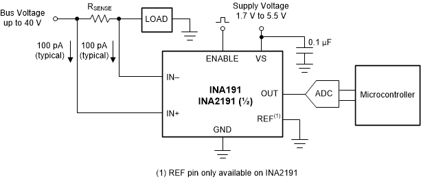
GUID-20210129-CA0I-H5N2-V2DZ-GJPBLMW0HCDV-low.gif Figure 8-1 Basic Connections for the INAx191

A power-supply bypass capacitor of at least 0.1 µF is required for proper operation. Applications with noisy or high-impedance power supplies may require additional decoupling capacitors to reject power-supply noise. Connect bypass capacitors close to the device pins.