ZHCSFN3E August 2006 – January 2021 INA193A-Q1 , INA194A-Q1 , INA195A-Q1 , INA196A-Q1 , INA197A-Q1 , INA198A-Q1
PRODUCTION DATA
- 1 特性
- 2 应用
- 3 说明
- 4 Revision History
- 5 Pin Configuration and Functions
- 6 Specifications
- 7 Detailed Description
- 8 Application and Implementation
- 9 Power Supply Recommendations
- 10Layout
- 11Device and Documentation Support
- 12Mechanical, Packaging, and Orderable Information
7.3.3 Inside the INA19xA
The INA19xA uses a new, unique, internal circuit topology that provides common mode range extending from –16 V to 80 V while operating from a single power supply. The common mode rejection in a classic instrumentation amplifier approach is limited by the requirement for accurate resistor matching. By converting the induced input voltage to a current, the INA19xA provides common mode rejection that is no longer a function of closely matched resistor values, providing the enhanced performance necessary for such a wide common mode range. A simplified diagram (see Figure 7-1) shows the basic circuit function. When the common mode voltage is positive, amplifier A2 is active.
The differential input voltage, VIN+ – VIN– applied across RS, is converted to a current through a 5-kΩ resistor. This current is converted back to a voltage through RL, and then amplified by the output buffer amplifier. When the common mode voltage is negative, amplifier A1 is active. The differential input voltage, VIN+ – VIN– applied across RS, is converted to a current through a 5-kΩ resistor. This current is sourced from a precision current mirror whose output is directed into RL, converting the signal back into a voltage and amplified by the output buffer amplifier. Patent-pending circuit architecture ensures smooth device operation, even during the transition period where both amplifiers A1 and A2 are active.
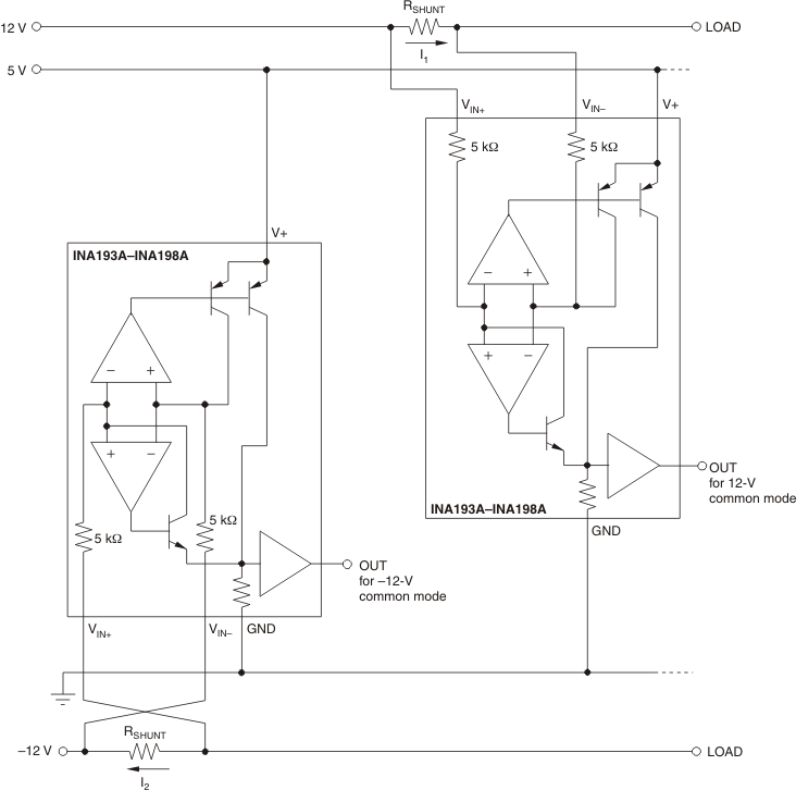
 Figure 7-2 Monitor Bipolar Output Power-Supply Current
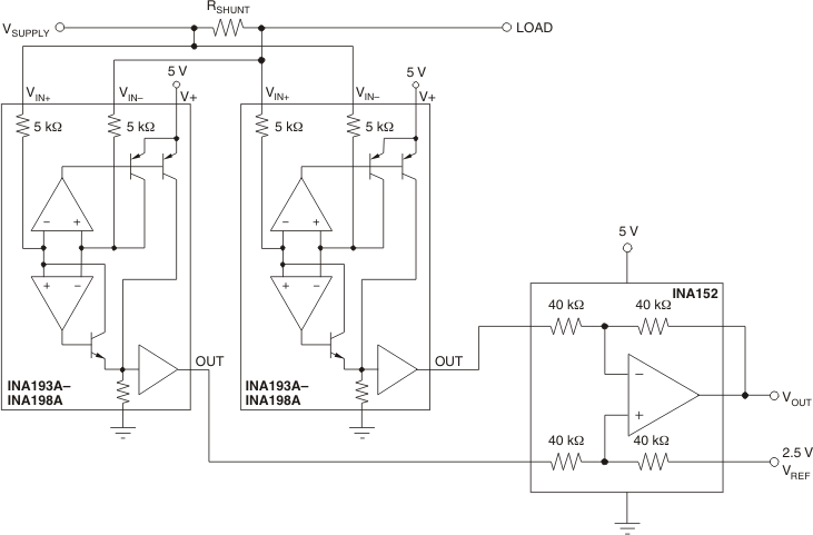
 Figure 7-3 Bidirectional Current Monitoring
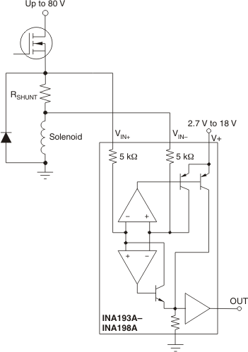
 Figure 7-4 Inductive Current Monitor Including Flyback
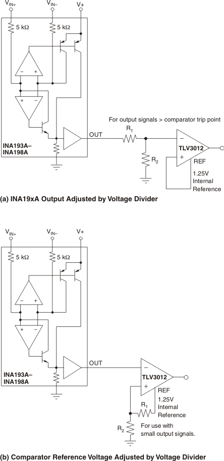
 Figure 7-5 INA19xA With Comparator